This thread has been locked.

If you have a related question, please click the "Ask a related question" button in the top right corner. The newly created question will be automatically linked to this question.

LM5022-Q1: Mosfet overheat at high frequency operation as boost

Part Number: LM5022-Q1
Other Parts Discussed in Thread: LM5022, LM5085

Hello,

I'm current designing a UPS that needs a booster to raise the voltage from 56V to 90V @ 5A output. 

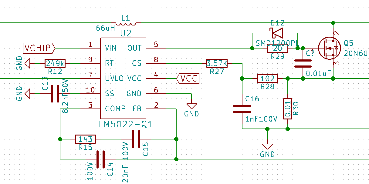
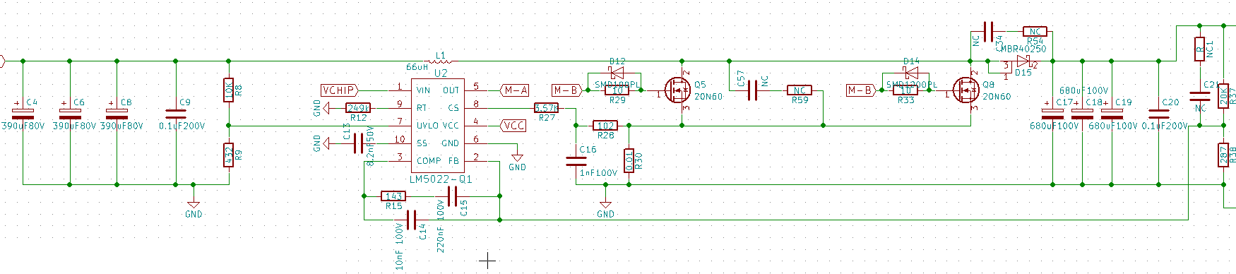
After studying a lot of the IC we picked up the LM5022-Q1 to use it as a boost converter.  We used the datasheet from the LM5022 to calculate all the componets and webench as reference.

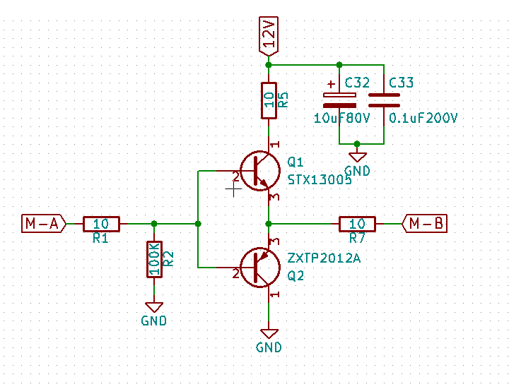
The problem we have is the mosfet is overheating when we operate at more than 2A Output at 200KHz. The mosfet we are using is 20N60 from Fairchild. To drive we use a totem pole with the transistors STX13005 and ZXTP2012A with with a 12V supply provided by a step down based in a LM5085.

As heatsink, it is be placed in a 60cmx45cm aluminum case with Gelpad and thermal paste.

If we change the switching freq to 60KHz we can get the output up to 5A but the output voltage drops to 79V at max output.

This is the circuit:

This is the mosfet driver:

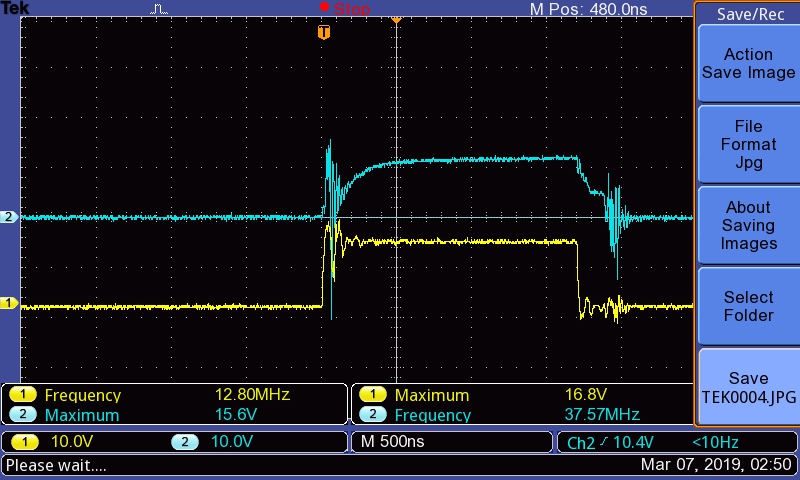
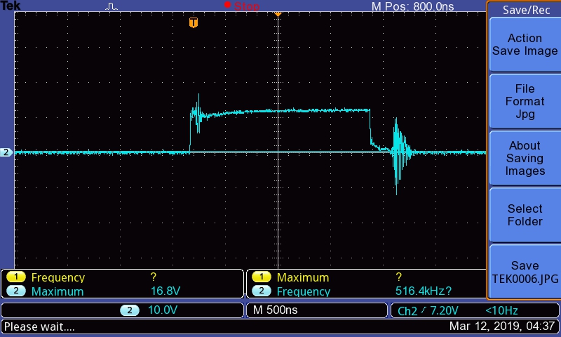
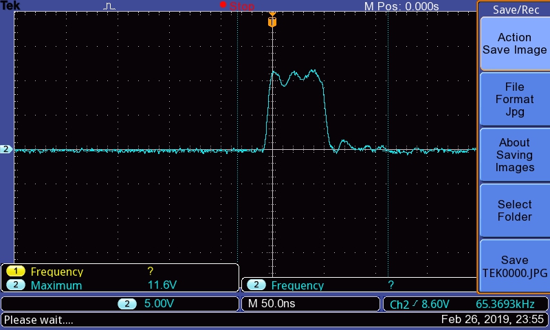
This is Output (PIN5) at no load operation:

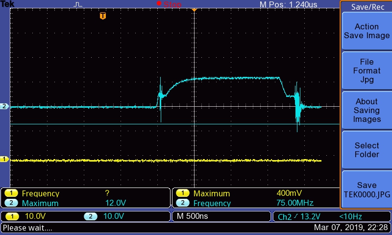
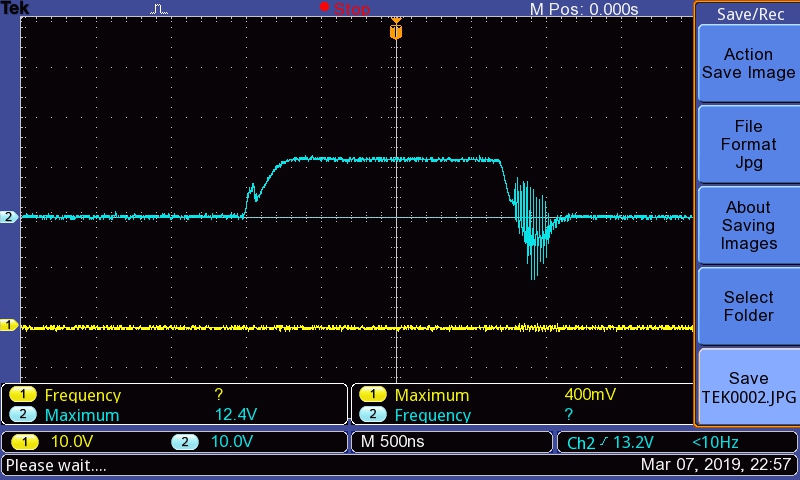
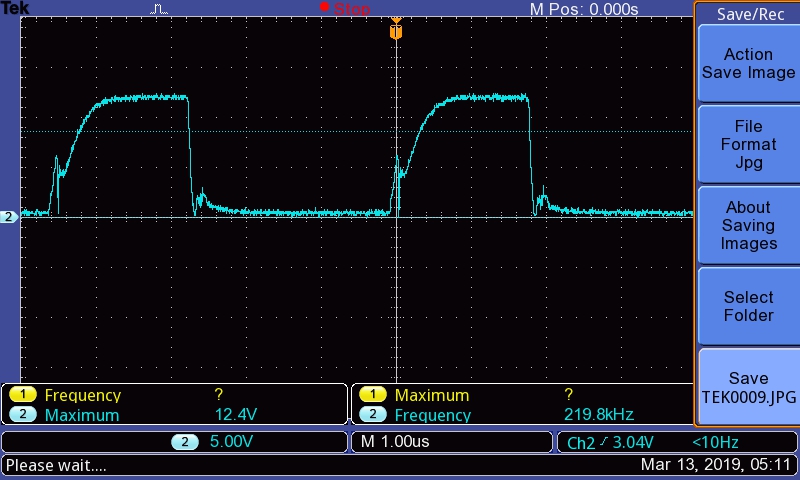
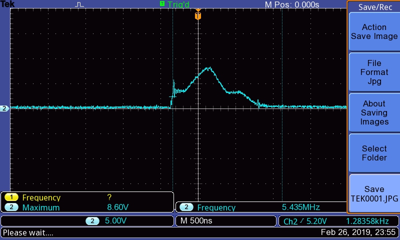
This is the GATE (After the totem pole)

Thank you very much in advance for your advice.

Kind regards,

Joel

  • Hi Joel,

    You can see from your MOSFET gate that the driver is not not very efficient. It should look like Pin5. Basically your totem pole bipolars do not have adquate HFE. Please replace these bipolars with high HFE devices, and you also need to short out R7 for faster turn-off. The 10 Ohm there slows down the turn off and causes high switching losses.

    Thanks,
    Youhao Xi, Applications Engineering
  • Hello.

    I will do the modifications you sugested.

    When you say high HFE, you suggest which values?

    Thank you very much in advance,

    Regards,

    Joel

  • Hi Joel,

    I mean >>1, If the HFE is 100, then the Ie and Ic would be 1% difference, meaning 1% error in the voltage regulation.

    Thanks,
    Youhao
  • Hello Mr. Youhao,

    I tried changing the BJT for BC337 and BC327 with the following result:

    Yellow is PIN5

    Blue is the GATE of the Mosfet.

    The voltage now is maintained (at 200KHZ) but the mosfet is still overheating.

    I removed R7 but I get too much ringing, so I reduced the R7 to 4.7ohm instead.

    Do you know what else might be the problem?

    Thank you very much in advance!

    Kind regards,

    Joel

  • The blue trace still has too much ringing, and it passes the gate threshold multiple times, causing unnecessary multiple switching. Also the turn-off transient look too long. Can you increase your gate resistor to 10 Ohm, and add a parallel diode to the resistor to speed up the turn-off transient? The diode anode should connect to the MOSFET gate, and the cathode to the IC driver pin.

    Thanks,
    Youhao
  • Hello Mr. Youhao,

    The gate resistor already has a schottky diode (SMD1200PL) for quick turn off.

    I added a capacitor between the G and the S to eliminate some of the ringing in the circuit.

    Before:

    After a 0.01uF Ceramic Capacitor between G and S.

    Without the turn on ringing the overheat slowed down and improved, but it still gets too hot to operate and the mosfet reaches over 100°C.

    I tried adding a Zener diode between the G and S trying to "clamp" the negative voltage with no results.

    Do you have another suggestion to eliminate the turn off ringing?

    Thank you very much in advance.

    Joel

  • Hi Joel,

    It seems the layout needs to be improved. We do not recommend to add a capacitor at the MOSFET gate.

    The main problem is in your external gate drive circuit which cannot efficiently drive the MOSFETs. Your R7 should be shorted (or 0 Ohm) because it slows down both turn-on and turn-off. You should also short R5 and replace it with a 0 Ohm.

    Let me know if you see any improvement.

    Thanks,
    Youhao
  • Sorry I mistakenly clicked TI Thinks Resolved. Please reopen this thread by following a new post.

    Thanks,
  • Dear Mr. YouHao,

    I shorted the driver and right now I'm driving the mosfet straight from the LM5022 with a 20 Ohm gate resistor and a schotty diode for discharge:

    VCC is 12V

    This is the waveform at Pin 5

    And this is at the gate with no driver and only the schotty diode and 20 ohm.

    Changing the resistor from Gate Resistor 20ohm to 10 ohm only damaged the 5022.

    I also tried adding a snubber for the mosfet but it did not work. The RC was 10Ohm 1nF.

    This is the Layout:

    Everything is super close in order to prevent any noise from entering the circuit.

    The Mosfets we are using are located on the left.

    The Inductor is in the upper part of right side and next to it, to the left, is the diode.

    Thank you very much in advance,

    Kind regards,

    Joel

  • The waveform shows a layout problem: there is remarkable parasitic inductance along the gate drive signal path, and the inductance causes ringings. Please help trace the drive signal from the IC pin 5 to the MOSFET Gate, then from the source through the CS sense resistor and back to IC GND pin. This will help us understand how to improve your layout to avoid the gate drive ringing.

    Thanks,
    Youhao
  • Dear mr Youhao,

    We changed the PCB for a new one (without any tests on it) and significantly improved the ringing problem.

    The thing is that we still get a thermal rundown in the mosfets as soon as we add a 4.5A load to it.

    This is the signal we have now:

    As for your previous suggestion, the mosfet source is connected almost directly to CS and to GND. As for the gate driving circuit it might be a long path.

    Do you have any other suggestion or waveform you want to check?

    Thank you very much in advance,

    Kind regards,

    Joel

  • Hi Joel,

    Youhao is out of the office. He will be back next Tuesday and should be able to support your questions.

    Thanks,

    Garrett
  • Hi Joel,

    Thank you for the updates, and the waveform is much better. Is this at the MOSFET gate? The rising edge is still slow and you may reduce your 10 ohm gate resistor R1, R5 and R7 to, say =2 Ohms, and see if the rising edge can be more faster.

    The rising edge also shows effects of trace inductance in the gate drive circuit. The most import paths are two:

    (1) the driver: your external driver output and return must be close to the IC and your should trace your driver current flow path and make sure it is direct, short and does not enclose large spatial area.
    (2) current sense: the CS signal should be directly from the CS resistor and the sense signal to the IC should be short, direct, and it does not enclose large spatial area with it return path from the IC gnd pin back to the CS resistor gnd pad.

    Thanks,
    Youhao
  • Dear Youhao,

    We have resolved to do another PCB with different current paths and also with a closer driver.

    We have another question regarding the IC, because it is noted that this should not work at a frequency less than 200Khz, but we were using it at 100Khz. Why cant you use this at a this frequency?

    Thank you very much in advance,

    Regards,

    Joel

  • Hi Joel,

    The device is qualified from 200kHz to 2MHz. It may work outside this range, but TI do not guarantee the operation and performance. Datasheet information is what TI can guarantee.

    Thanks,
    Youhao