This thread has been locked.

If you have a related question, please click the "Ask a related question" button in the top right corner. The newly created question will be automatically linked to this question.

UCC21520-Q1: Input Current IVCCI Curve & Max?

Part Number: UCC21520-Q1

Hi team,

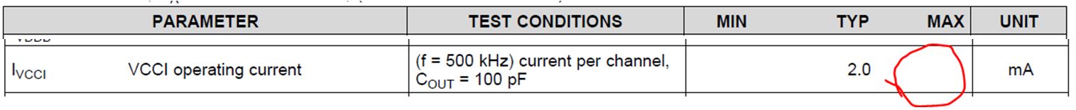
Q1 - is there a max value specified for IVCCI in operating? Only typical value is specified. 

Q2 - in datasheet, typical IVCCI is specified at 2.0mA under test conditions of "(f = 500 kHz) current per channel, COUT = 100 pF" ==> can elaborate? is this condition under 0 output current with freq = 500kHz? 

Q3 - is below curve referring to IVCCI or IVDDA/IVDDB? 

  • HI PengYu,

    Thanks for reaching out to us, my name is Mamadou DIallo, I will help address your question.

    Q1- IVCCI(max) is not specified but should not vary by a big margin.

    Q2- IVCCI or "operating current" is the VCCI current consumption (per channel) when a 500kHz PWM input signal is applied to ChA/B with a load capacitor (100pF in this case) at the output which is different from quiescent current when the VINA = VINB = 0V and no load connected.

    Q3- Figure 4 represents variation of the operating current IVDDA/B over frequency at NO LOAD.

    Please let us know if you further questions.

    Regards,

    -Mamadou
  • Hi Mamadou,

    Q1 - do we have any estimation on this? 

    Q2 - will IVCCI vary with PWM frequency? do we expect a higher IVCCI when input PWM frequency increases? Is there a curve to show the correlation? 

    Q3 - clear. 

    bottom line is how to estimate the max IVCCI based on application condition. can you let me know what are the parameters (like VCC, PWM freq, temperature etc) required to estimate (if not to guarantee) the max IVCCI? so customer can design the power supply based on this worst case. I can gather those parameters from customer. 

  • Hi PengYu,

    In the section 9.2.2.4 of d/s, we have 2.5mA of switching IVCCI at no load at 100kHz.

    As you may notice in the same section, the gate driver losses contribution will mostly be dominated by VDDA/B and IVDDA/B. I would expect variation in IVCCI based on VCC, frequency and temperature but those variations should not exceed +/-10mA (rough estimate).

    I will check Monday and get back to you for any possible approximate IVCCI data that was previously done on this device.

    Thanks for your patience.

    Regards,

    -Mamadou
  • Hi Pengyu,

    I am still working on your request, I will get back to you by EOB Wednesday.

    Thanks.
  • Hi Pengyu,

    The input current increases when an input is set HIGH and the device is transmitting in its ON state, independent of actual PWM frequency. This device has two transmitters, each consuming between 0.8-mA and 1-mA when asserted high at 100% duty cycle. This value changes slightly over temperature and process.

    Input RMS current scales proportionally with duty cycle when the inputs are driven by a PWM signal. It can be estimated as 1-mA * D, for each channel. For example, if the inputs of this two-channel driver are driven with a complementary signal of any particular duty cycle, the RMS current will increase by about 1-mA. If the DT pin is shorted to VCCI to deactivate the feature, and both inputs are driven high, each transmitter will consume ~1-mA and total input current will increase by 2-mA. The datasheet lists the typical input current for a 500-kHz, 50% duty cycle complementary signal on the inputs.

    The DT pin can also add to increased input current if it is programmed with a resistor. The DT pin voltage is nominally 0.8-V. The additional quiescent current is approximately 0.8-V/RDT. This approximation only holds true with larger resistor sizes; if DT is shorted to GND, it will add around 1.5-mA. 

    If this helped answer your question, could you please press the green button?

    If not, feel free to ask for more clarification.

    Thanks and best regards,

    John

  • Hi,

    The question is what is the worst case maximum IVCCI? Understand we may not guarantee this parameter as it is not specified in the datasheet, but can we have a reasonable estimation or simulation of this parameter? Like up to  +50% to 3mA? up to 10 times to 20mA? up to 200 mA? etc 

  • Hi PengYu,

    The worst case maximum IVCCI is approximately 5mA. This condition assumes operating at 5V, DT shorted to GND, one input shorted high, the other input shorted low.

    Thanks,
    John
  • Hi John,

    Is 5mA worst case for 2 channel operation with one channel short or both channel short?

    Do you have worst case current for 2 channel normal operation?

  • Hi Pengyu,

    5mA is worst case for 1 Channel operation with the DT pin shorted to GND, and is the highest expected input current for any configuration.

    The worst case for 2 channel operation would be with DT tied to VCCI, and both inputs high at 100% duty cycle. This would require approximately 4.5-mA.

    Thanks and best regards,

    John

  • Hi John,

    is the 5mA (4.5mA) referring to the input current, OR the supply current? I need to know the max supply current from VCC (IVCCI).
  • Hi Pengyu,

    The 5-mA/4.5-mA refers to the supply current going into the IVCCI pin (pins 3 and 8). The input current to INA and INB will be much smaller.

    Thanks,
    John