This thread has been locked.

If you have a related question, please click the "Ask a related question" button in the top right corner. The newly created question will be automatically linked to this question.

TPS24700: Schematic Review

Part Number: TPS24700
Other Parts Discussed in Thread: CSD19533Q5A, CSD16415Q5

Dear Team,

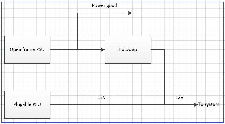
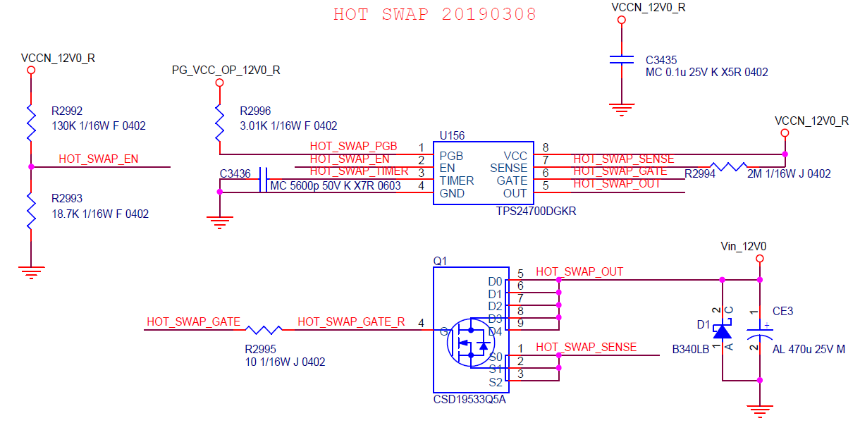
Can you help on the schematic review?

I already checked it, but I may need your double confirm.

Attached the MOS and excel tool

EDM000011097800.pdf

8358.TPS2470x_Design_Calculator_Rev-.xlsx

BR

Kevin

  • BTW, the only information engineer have is Vin=12V, Iin=8.3A
    They just want to use this circuit for enable function.
  • Hi Kevin,

    I will review this and get back to you by tomorrow.
  • Hi Kevin,

    Looks like there are some basic mistakes in the schematic,

    • Source of the mosfet is connected to sense resistor and the Drain of the Mosfet is connected to Output Capacitors. This will make the body diode conduct whenever Vin is present and the controller is disabled. The Drain and Source connections have to be interchanged.
    • Sense resistor used seems to be 0402 and 1/16W. The sense resistor power rating needs to be at least 150% of the calculated power loss in the Sense resistor. 

    Also, the calculator seems not to have the correct values loaded,

    • The Output capacitance in schematic is 470uF but the calculator shows only 68uF
    • The FET in the schematic and Calculator are not the same.

    Please share the  calculator with correct values loaded as per specification and matching the schematic. 

  • Dear Praveen,

    I will ask the customer to provide the new schematic soon.

    pony.xlsx

    Here is the new excel tool I input, sorry I didn't check the customer excel tool first.

    May I know some parameter on how to design?

    Iramp Choose output capacitor charge current (<Plim/Vccmax)
    RLOAD-start Resistive load present at start up (must be > RMIN-start)

    Cgate Gate capacitance for dV/dT control

    Should I ask the customer to put a place holder cap for Cgate?

    SOA_mrg SOA margin -14.8

    It mentions negative SOA margin, is it acceptable?

    BR

    Kevin

  • Hi Kevin,

    Since this is a 12V application, you can ask customer to consider using a  low voltage (30V) FET to get better Rdson. 

    Please see my response below on design calculator,

    • Iramp: This is the current with which you would like to charge the Output capacitors.  This will decide the dV/dT of the output voltage for a specific Output Capacitance.
    • RLOAD-start: This is the effective load which can be modelled as a resistor during startup.  Generally, we recommend to have no load during startup because it reduces the startup time and reduces the stress on the FET during startup.
    • Cgate:This is the external capacitance placed at gate of the FETs for dV/dT based startup. This value can be the closest value to 'Cgatec'(which is the cell above Cgate in design calculator). It is better that customer places a place holder for Cgate. 
    • It is required to have at least 20% SOA Margin. but we recommend an SOA margin >30%.  If the SOA margin is not >20% try choosing a FET with better SOA, less gate charge (FET Gate Charge to reach Vgs > Vta (single FET)). 

  • Dear Praveen,

    Thanks for the information.

    How much will the capacitance you will suggest to put between Gate pin and resistor?

    I think the circuit looks good now, do you have further suggestions?

    BR

    Kevin

  • Dear Parveen,

    The purpose of adding hot swap on the schematic is to make the open frame PSU have a PG signal (block diagram is as follows), then please help us to see if there is any need to adjust our schematic.

    BR

    Kevin

  • Hi Kevin,

    Please send the final schematic and design calculator for review. The schematics cannot be validated without the design calculator as we need to check if the FET can support the design specification.
    In your system, do you intend to use the PG signal from TPS24700 to control your down stream loads ? Sorry I did not get from the block diagram how you are generating the PG signal before Hotswap.
  • Dear Parveen,

    Please have a look of excel file and SCH.

    Because the hot-swap input is from the power supply, which has a softstart function. 

    So the MOSFET SOA is not that important, right?

    I think the block diagram should move the power good after the hot-swap, which make more sense here

    Hotswap SCH.pdf

    0523.pony.xlsx

  • Hi Kevin,

    Please see my comments below,

    • The  schematic and Design calculator you shared still have different FET's. the schematic shows  CSD19533Q5A but design calculator has DMT34M1LPS. The SOA of DMT34M1LPS is not good enough. This is the reason why you see the SOA as 'FAIL' in the design calculator. So, the design is not recommended with DMT34M1LPS.
    • I have updated the design calculator and attached here with CSD16415Q5. You can see that the  SOA Margin is 74% with CSD16415Q5. You can consider using this FET .
    • Also use a Sense resistor with higher power rating.  Make sure you at least have 50% margin in power rating of the sense resistor.
    • We recommend using a TVS at the input of the  Hotswap to clamp the  inductive kickback voltage during turn OFF of the  FET.
    • Change the Ctimer as per Design CalculatorPraveen Edited.xlsx