This thread has been locked.

If you have a related question, please click the "Ask a related question" button in the top right corner. The newly created question will be automatically linked to this question.

LM3524D: LM3524D Closing the Voltage Feedback Problem - the Output Phase Shifts Uncontrolled

Part Number: LM3524D
Other Parts Discussed in Thread: SG3524

Hello,


I am having troubles closing the voltage feedback loop from the output to the inverting input of the error amplifier, pin1 of LM3524D. As soon as I feedback enough signal such that the IC starts to regulate, I get intolerable phase shifts of the two outputs signals and as a the MOSFETs burn out over time.


The IC is driving a pair of MOSFETs (through MCP1407 drivers in between) in a push-pull configuration with two primary windings centered at 12V. Circuit converts around 500W power from 12V to 51V DC (unfiltered) at 4.8Ohms and works as it should, very stable, no issues there.


The problem is such as, as soon as the signal from the output is so high enough that the IC is starting to regulate the output, which it does, the two outputs from the LM3524D start to phase shift very rapidly. With this kind of signal, it doesn’t take too long for the MOSFET to burn out.


I am using a 50kOhm potentiometer to feed back the output to pin 1. Also pin 1 is coupled to GND by a 100nF which forms a RC filter together with the Potentiometer.


When I investigated further, the triangular voltage generated at pin 7 (Ct) also phase shifts in the same pattern like the MOSFET signals, which appears to be the reason for the problem.


I have uploaded a short 34 second video showing on the oscilloscope the problem:

https://youtu.be/ulSgwuk_lk0


Do you have a tip on how to resolve the damaging for the MOSFETs phase shifted signals? Thanks for any help

  • Hi Ivaylo,

    Thanks for posting the video, it was really useful.

    The first thing I suggest is that you need to re assemble the circuit with much shorter and neater connections. With the current construction it is highly probable that the dv/dt from the switching edges will couple into the control signals and cause all sorts of issues.

    I also suggest you try and run the IC open loop first by connecting the voltage error amplifier as a unity gain follower and putting an adjustable DC voltage source on the non-inverting input to vary the compensation voltage level directly.

    If you can get clean operation in open loop you have some chance of getting good performance once you close the control loop.

    Regards

    Peter
  • Thank you @Peter Meaney for giving a hand. I haven't had really much time to wotk on it since my SMPS went down, an inrush 12A NTC is blown apart. Maybe I should increase the time constant on pin 9 for softer start. From the couple minutes time i had to test with new (16A) drivers and reducing the gain of the amp I already saw some imrovement from each of both measures. I need to find a NTC replacement and start testing, or get a mighty car battery :) 

  • Hi Ivaylo,

    I hope you have made some more progress in the meantime, I am going to close this post. Please open a new post if you have more questions.

    Regards

    Peter
  • Hello Peter,

    I am fixing my SMPS and I got message that my order with the couple of 650V MOSFETs together with Power Schottkys and NTCs have just arrived. I will fixing it on Monday and right after that I am up and running with tests with SG3524. Please do not close this thread, is it possible? Thank you in advance! Ivaylo 

  • I have already repaired the SMPS, changed three blown MOSFETs and a very fast recovery Schottky together with the NTC. Power supply works as new and I've made some measurements.  

    Phase shifting  was still there and noises were coming from the trafo. I hadn't have isolation between the primary and the secondary winding and that is what actually fixed say one half of the phase issues. Phase shift appears only on no load and is less than before.

    PWM regulation with full voltage feedback works yes finally,  full load voltage 46.5V. Without a load voltage increases upto 48.5V and PWM intervenes accordingly all this with a 1Meg resistor between pin 9 and pin 1.

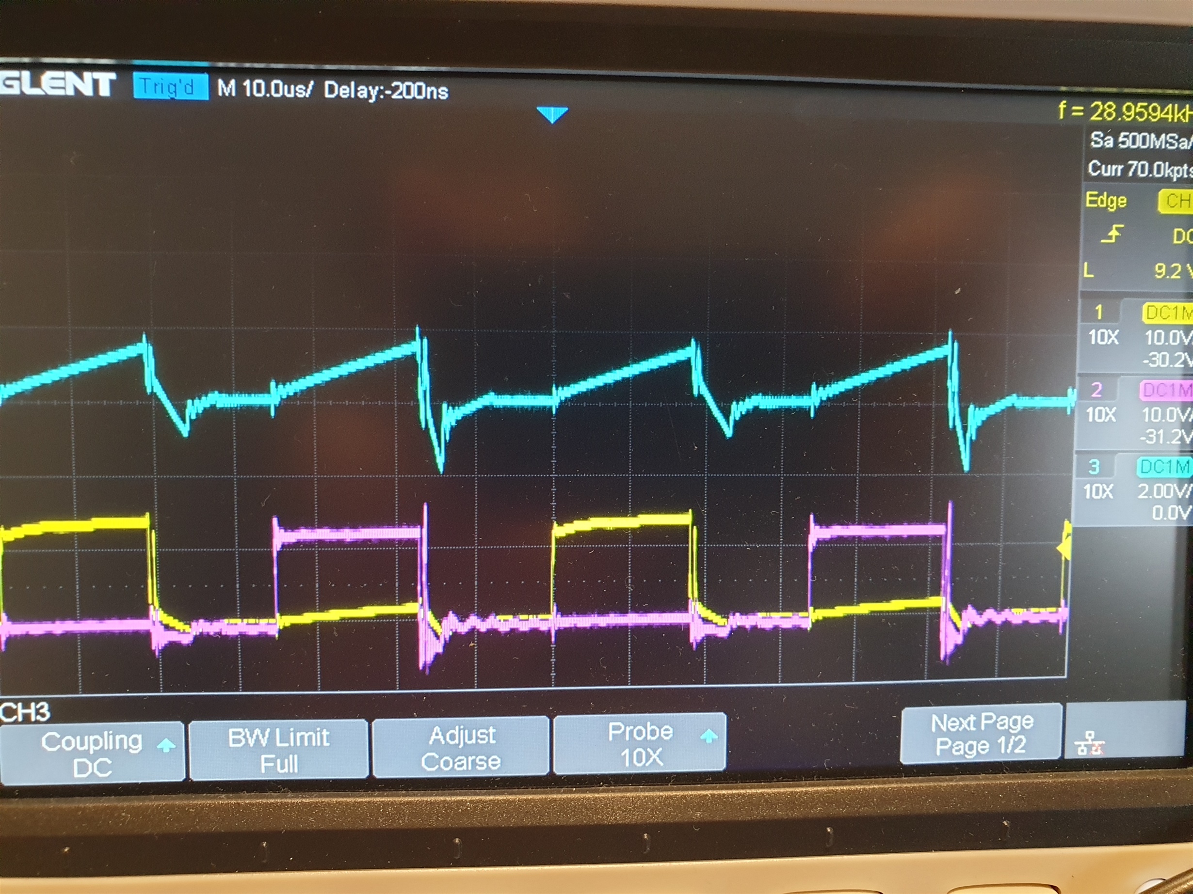
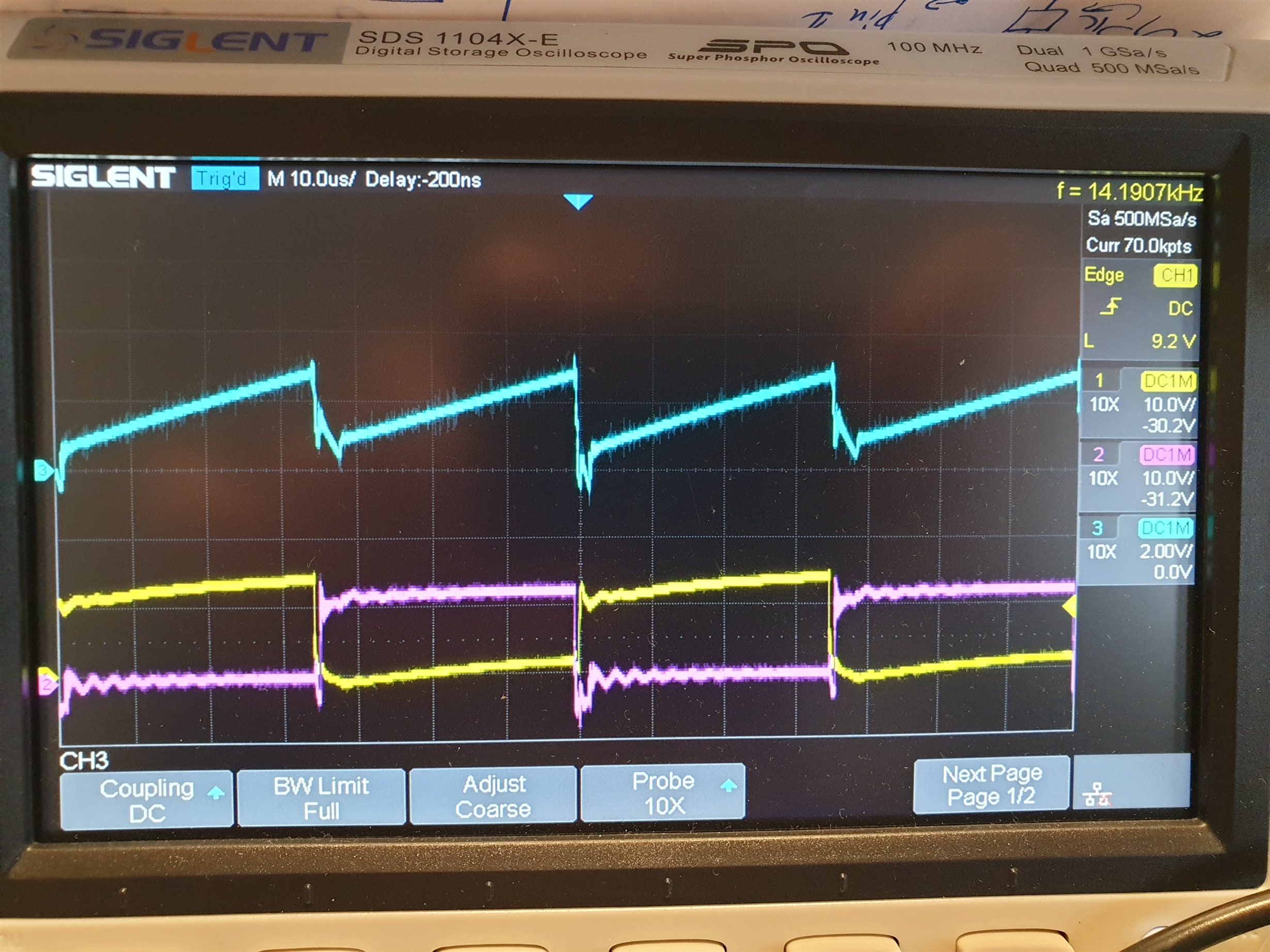
    I made current measurements with a specialized 100A oscilloscope sensor (2 MHz bandwidth), the osci graph in blue. There are things i connot explain..

    So 1V corresponds to 40A, 1st picture is with no load and 2nd one with 4.8 Ohm load (voltage is 46.5V). First picture shows 28kHz because of the phase shifts (appearing only at no load)

    How is it possible for the current to flow in the opposite direction after the MOSFETs are off (blue graph below the zero line). This negative current also differs with factor of 2 between the two MOSFETs. Is it a resonance effect with the equivalent capacitor on the output of the SMPS? Also on the second picture with load, the current through the one MOSFET never reaches zero so currents overlap in spite of the dead time..

    How to explain this fenomena? 

  • Hi Ivaylo,

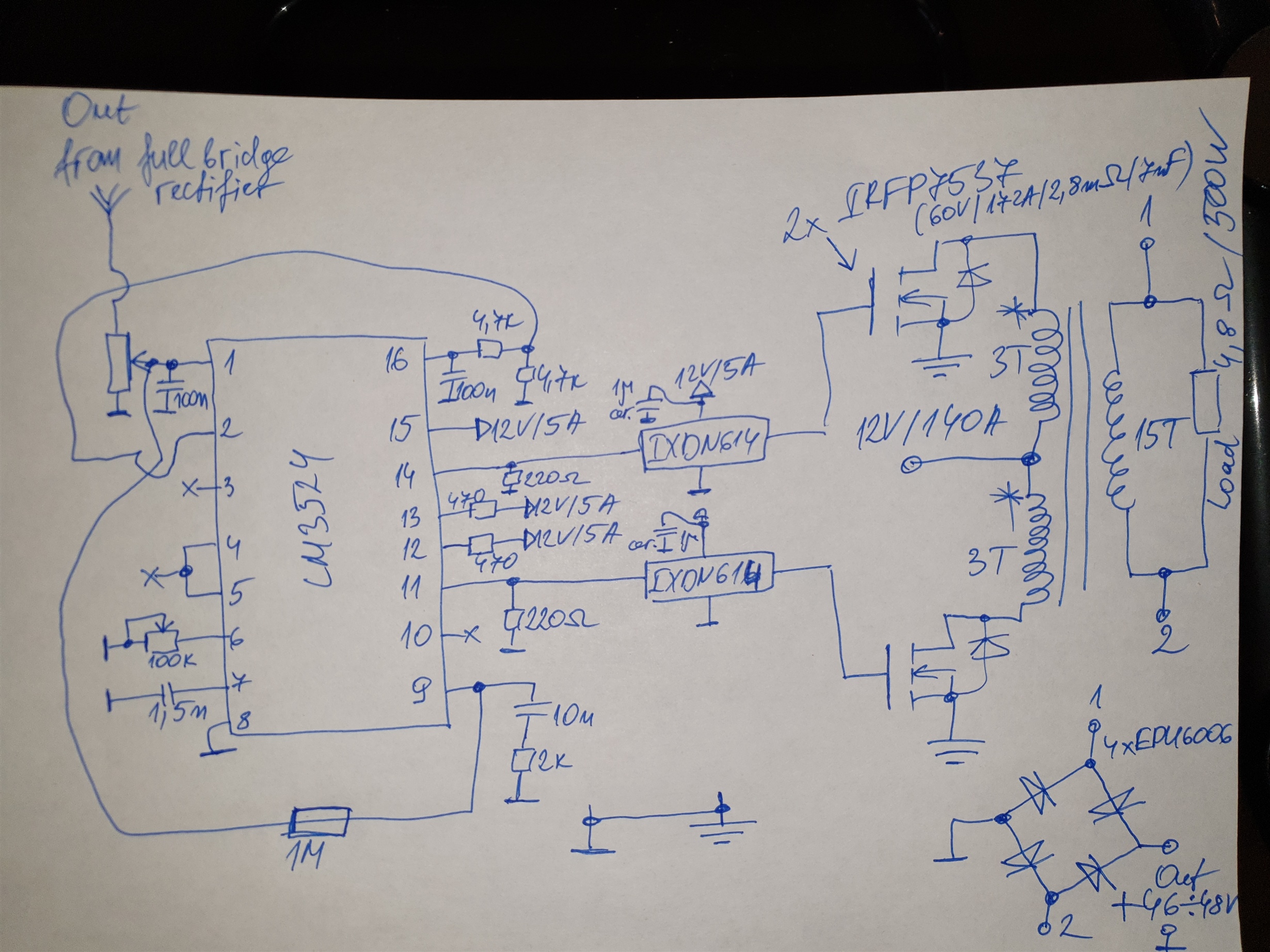
    Can you share your schematic and the transformer drawing showing the number of turns and winding layer arrangement?

    Thanks

    Peter
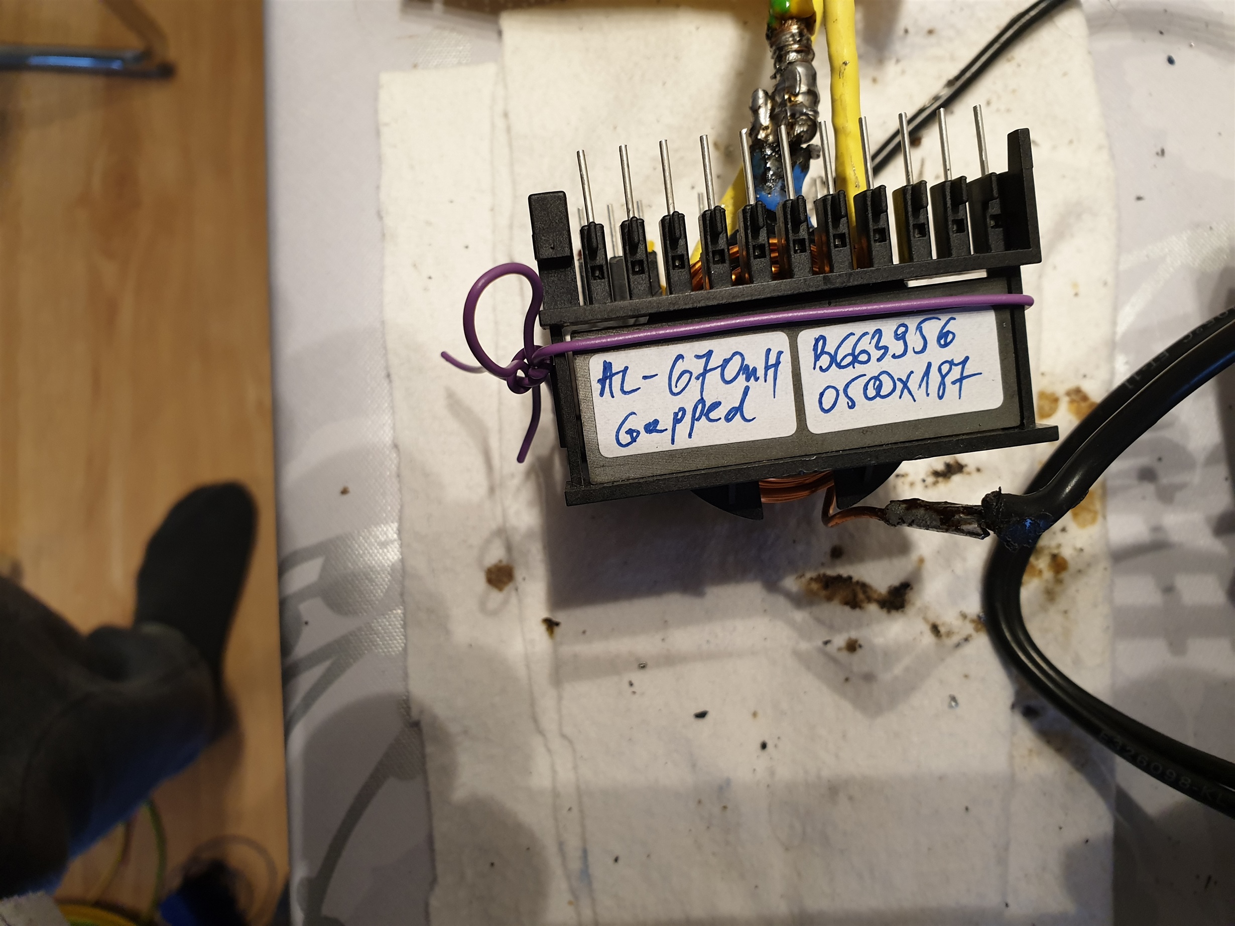
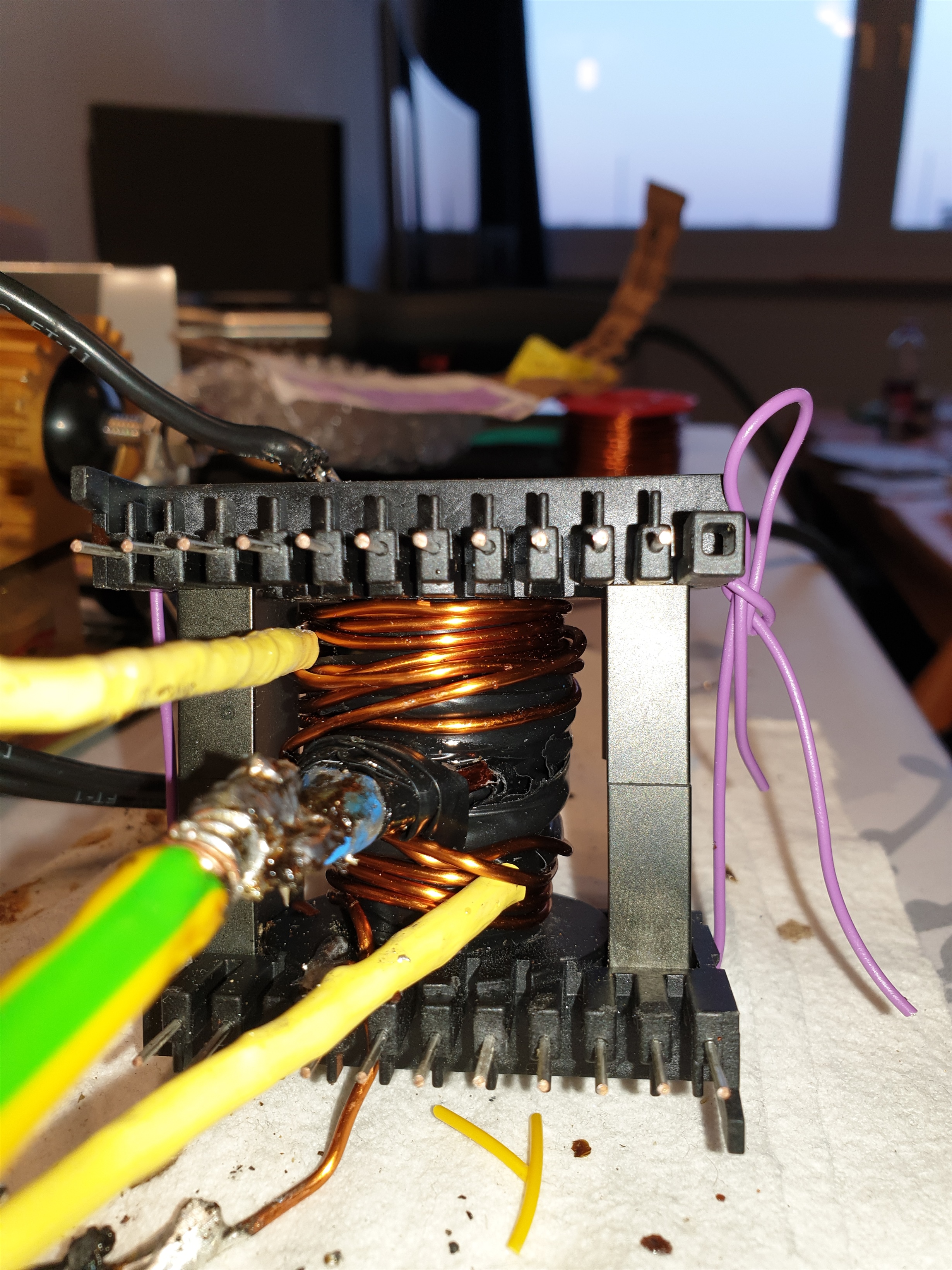
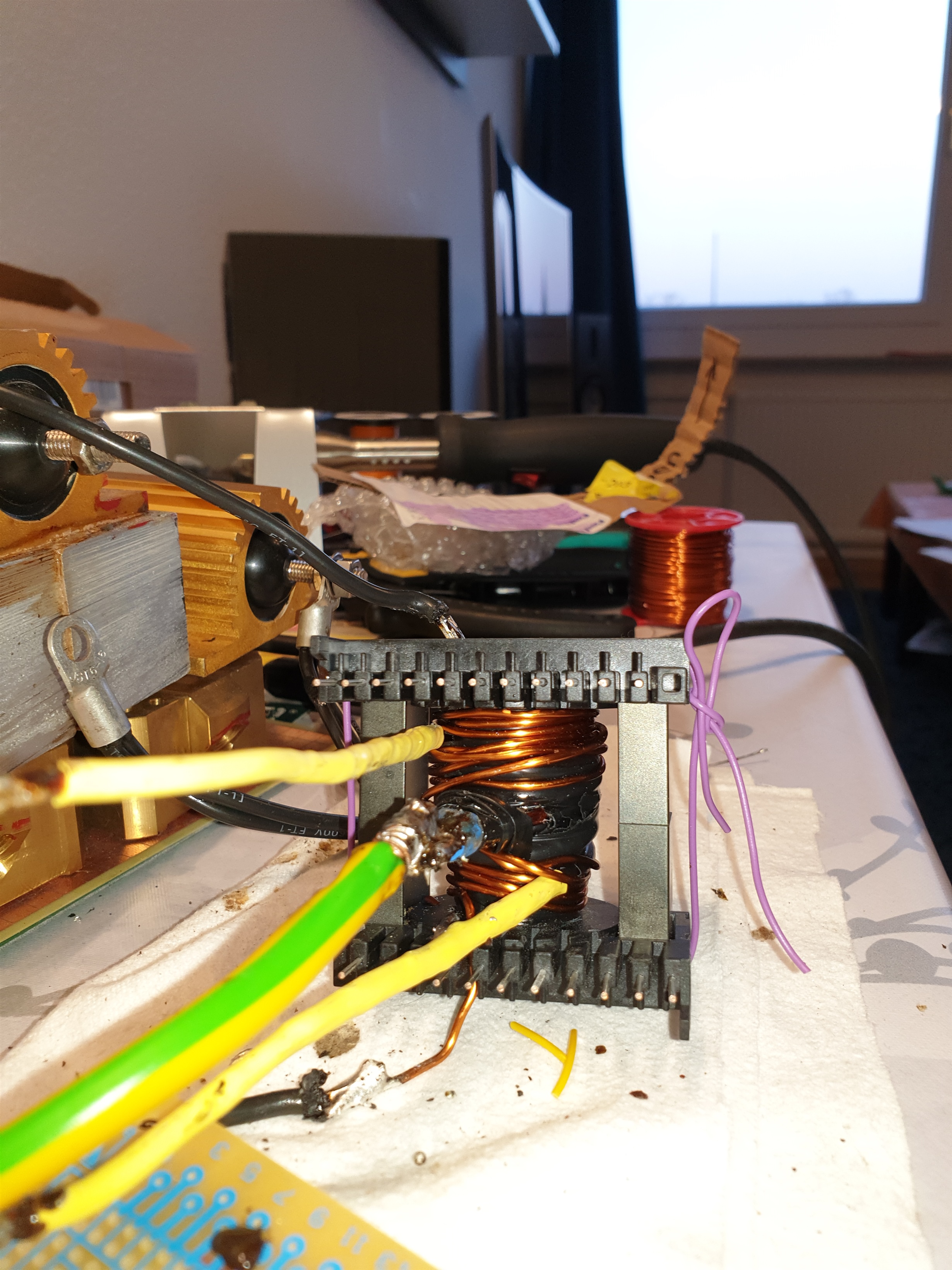
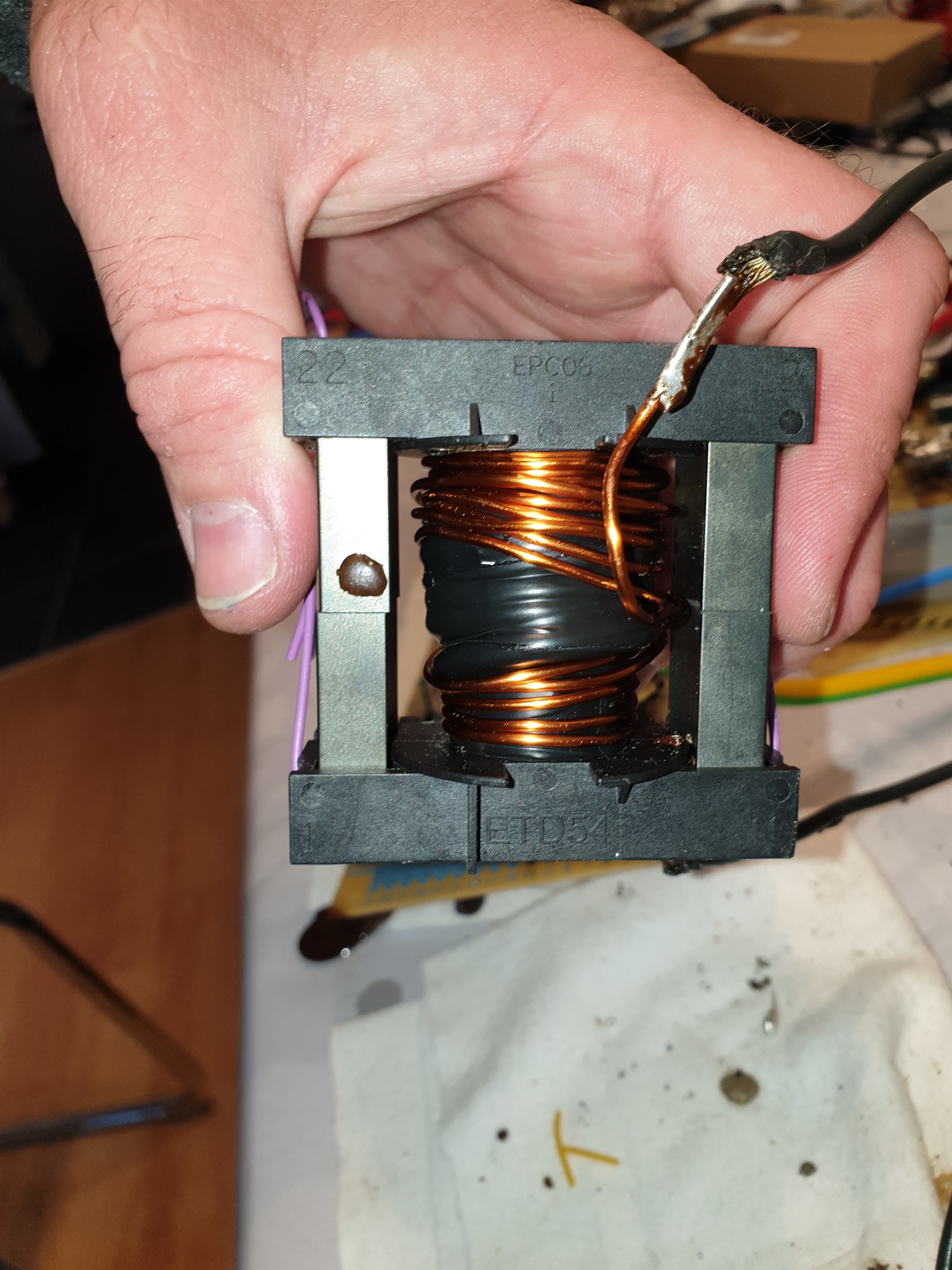
  • Thanks Pete for giving a hand, here are some fotos from trafo and schematics..

    There are now layers of isolation between the two primaries and the secondary comprising of electrical isolation tape. The vertical section of the coils where contacts are made (and where tape cannot be applied) are isolated by means of shrink tubings. Also potentiometer at pin 1 is 50k. Moreover LM3524 has a bypass cap of 470nF (not shown in the schematics). Furthermore rectifier is placed after the load so i don't have to be concerned with thermals on the schottkys at this point. The copper turns visible on the fotos are the turns of the secondary winding. Primary to secondary ratio is 2x3 turns : 1x15 turns

  •  Hi Ivaylo,

    Thanks for the schematic and the images of the transformer. Normally all the components, controller, gate drive IC, power mosfets and transformer are located on one PCB and a lot of effort is made to ensure that any connection with a switching waveforms or one carried high di/dt currents are as short as possible.

    It will be virtually impossible to get this circuit working with flying wire interconnections.

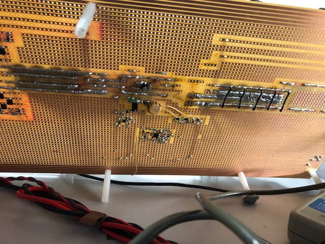
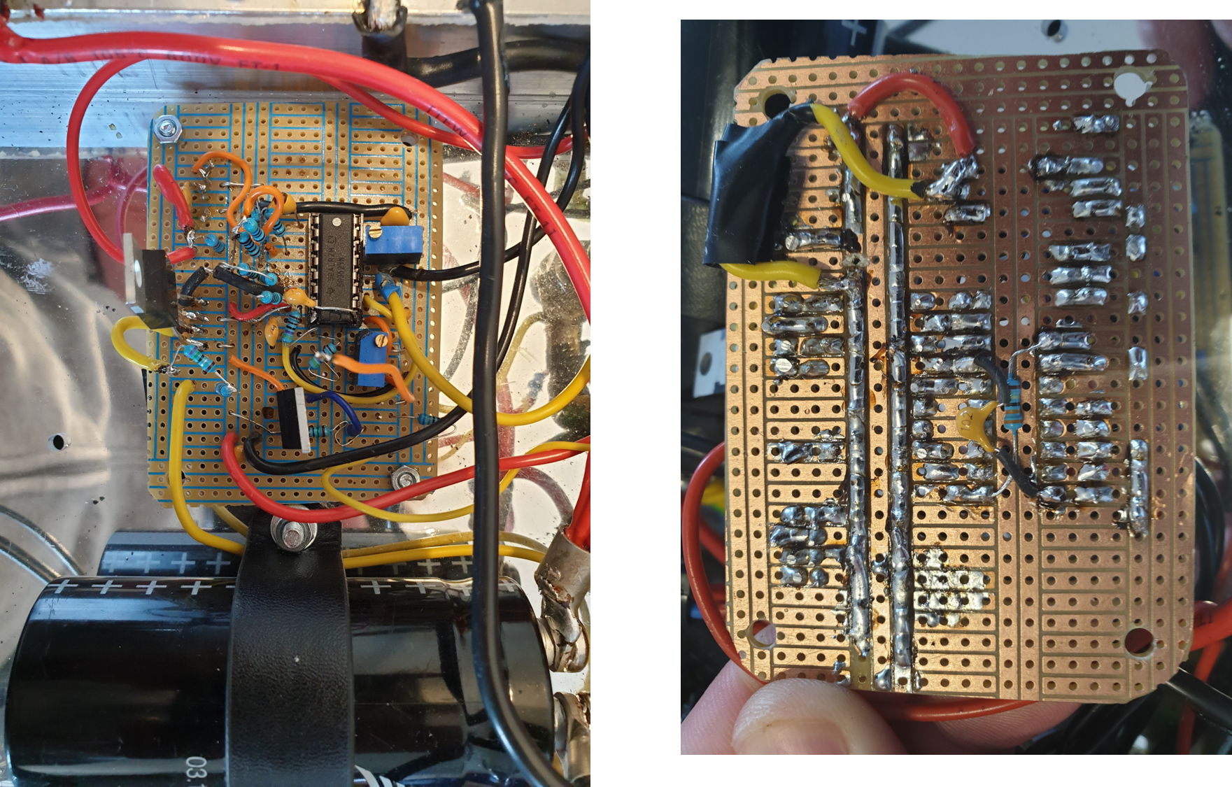
    I have included some images of a prototype board that we have in the lab for comparison.

    I also suggest you wind the transformer with multiple strands of wire in parallel to make the winding easier. I don't know what level of insulation the final application requires but general purpose electrical tape is ok for functional insulation for bench debug and may be degrade when hot.

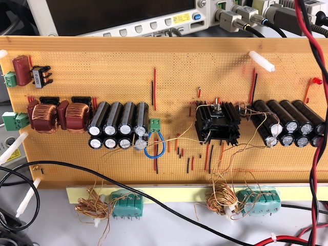
  • Thank you Pete i totally see the benefit of short connections, such as reducing the length of basicly antennas and even at 14kHz, the di/dt component can be quite high and causing those phenomena. In the meantime, i have achieved a phase-shifted free operation. It wasn’t quite the length but actually as it seems to me the di/dt component, but bear with me a little bit. Developing this circuit definitely takes a tow on wasted power MOSFETs and lot of hours but at the end it was worth it.


    As it phase shifted on no load only, I had my eyes on the transformer. I wasn’t happy with the, as we can see from the current sensor graph, at an average value of almost 20A supply current with no load, which amounts to a 240W of wasted energy. What I did is I completely rearranged the trafo. I increased from 2x3 to 2x5 windings on the primary and put extensive layers of isolation between the primaries and the secondary and pushed the trafo window size to its limit. Also I increased the frequency from 14kHz to 25kHz. As a result DC current at no load dropped 8 fold down to 2.5A with perfect gate signals. Since then I also removed the low ampere 12V supply completely and supplied the control circuit also from the 12V/140A line. I have enjoyed long minutes maybe an hour of 100% phase shifted-free operation with load and without. As result of the higher frequency and higher inductance of the primary I am getting somewhat lower voltage - but by no stretch of the immagination too low output voltage, 45V (compared to 46.5V to previous trafo configuration) with load (Resistive 4.8 Ohm) or 420W and full PWM stretch and 48.5V with no load, pwm at near 12%. As it turned out also this time, the trafo tweaks directly influenced the phase shifts, the difference is like night and day.

    Now the only remaining thing to do is to place the rectifier as it should be between the secondary and the load. Synchronous rectification I will not do, but a good old Schottky bridge will suffice and will post after tests shortly.

  • Hi Ivaylo,

    Just a note of caution when working at high powers, at the input side the current is 140A, the conduction losses in any interconnecting cables or connectors can be high and they will be hot. Power is I squared by resistance, 140A squared by 1mR is 19.6W!

    Make sure there is no combustible material near your setup.

    Regards

    Peter

  • Hi Ivaylo,

    Any updates?

    Thanks

    Peter
  • Hi Ivaylo,

    I hope you have made some progress in the meantime, since there has been no activity on this post I am going to close it. Please open a new post if you have more questions.

    Regards

    Peter
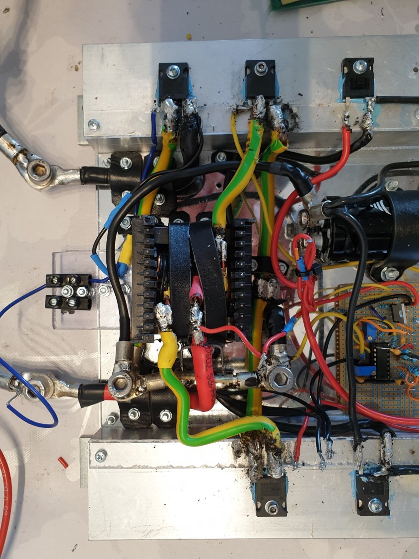
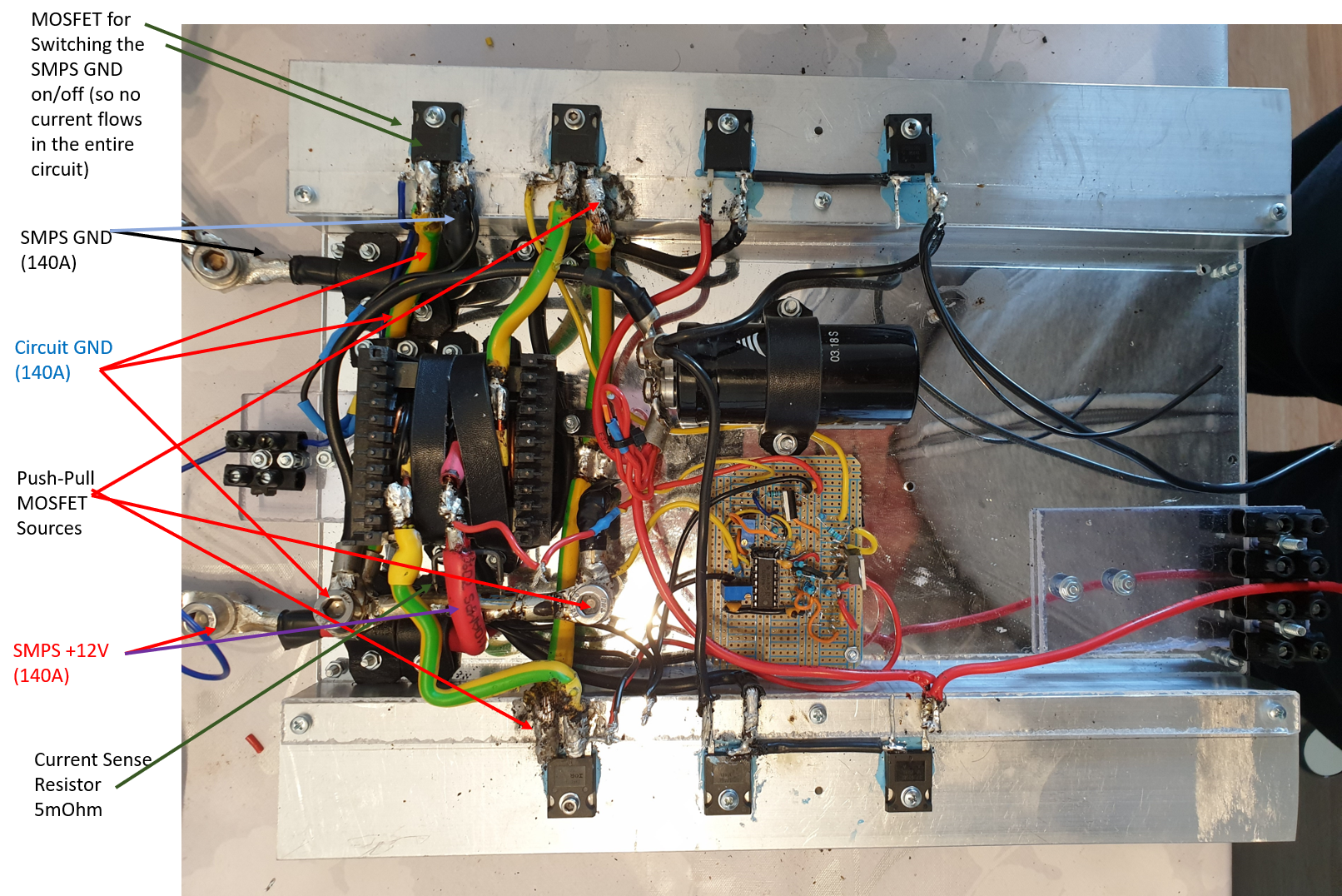
  • After achieving a steady state with the feedback closed with no shifting issues I have been working on the project and built a much smaller PCB, new heat dissipating contruction with short connections also power connections much shorter than before. The problem am experiencing is the new setup threw me backwards in the development. Not only i cannot close the feedback (burning mosfets) but i cannot even supply the SG3524 from the same power 12V/140A line, i am forced to use the separate 12V supply for it (with common ground), otherwise uncomtrolled phase shifts and mosfets are being burned. I have a question, the SG3524 has been for some time now. Are new controllers actually more stable, are there stabilty tests between the ICs?

  • Hi Ivaylo,

    There are newer controllers but the problem is not related to the control IC, I suspect the ground connection to the IC is been corrupted by high currents flowing in the return, negative input connection.

    If you have an input filter capacitor please take a separate connection from the negative terminal of the cap to the controller and then add 10uF of ceramic decoupling capacitor across the Vcc pin of the IC.

    Regards

    Peter
  • Hi Peter,

    I couldnt test because i am waiting for gate drivers. I have a 470nF, on pcb top side, the cap a bit covered by the red and black cables (IC Supply); near the big black capacitor 4700uF. As soon as i receive the drivers, i will test and try with the 10uF.

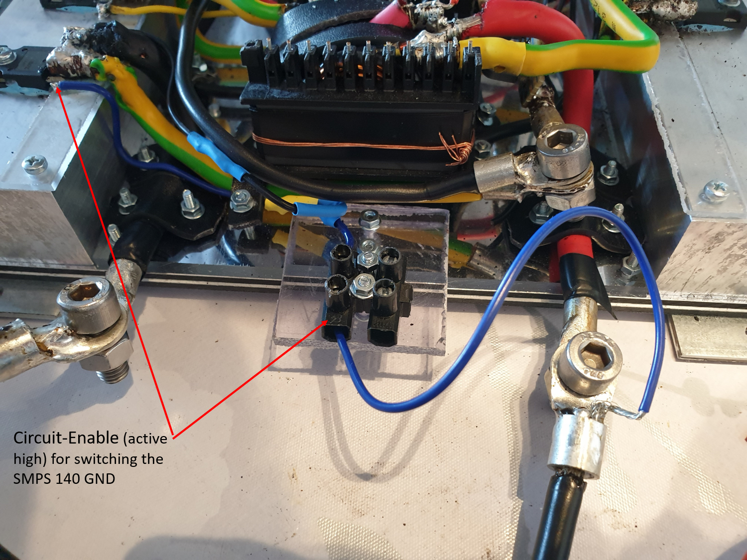
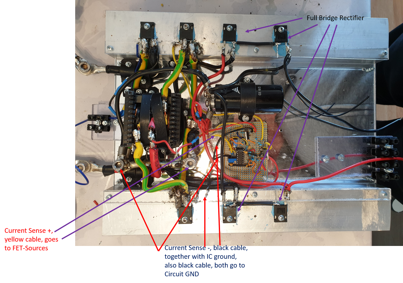
    In the meantime i have made some fotos with the new pcb and construction i have done, all connections a minimized in length please see fotos. 

  • I received my 16A (peak curent) drivers IXDN614CI but they turned out to be a huge dissapointment. Very easy to burn with the phase shifts, 6 pieces gone in a matter of a day. Also mounting them on a heatsink (TO-220-5) didnt solve the issue, so they were not burning because of excess power. They were gone even with 10Ohms in series with output, therefore burning not because of excess current. Those phase shifts were tourturing them bad. And along with them also several MOSFETs. I was having a rough time..

    I rather burn semiconductors, spend some money and learn something in the process. I found a soulution. So as it turns out, I built my own drivers with discrete BJT transistors (TO-220-3). Not even breaking a sweat, they work like a charm. I needed to boost for some du/dt at the edges and therefore used a parallel 150nF cap alongside the resistor between the IC outputs and the bases of the BJT driver (NPN-PNP stage).

    Now i could focus on those persistent phase shifts. I did a high frequency compensation of the error amp. Connected a 1nF cap between the output and the inverting input. Big difference. Now i was able to continuously run at high power, around 450W, without burning FETS. To be noted still with separate power supplies, one 12V/140A for the power and 12A/5A for the SG3524 pcb.

    As soon as I removed the 12/5A supply and connected the IC board on the 12V/140A supply, MOSFETs were giving up. Then I noticed something, with increasing the frequency the phase shifts get less and less pronounced. Unfortunately my output voltage under max load goes down. I thought “it’s the inrush current. I need to restrict it…”. I found an EMI suppression inductor laying around together with a 2.2uF X2 suppression cap. Connected those in a single stage LC-Filter before the center of the primary and voilà!!! Phase shifts were considerably less, I thought. No they were absent, my oscilloscope was having difficulty triggering the signals with those intense RF residue on the gate signals. With some playing with the trigger I attained this:

    https://youtu.be/zwGdumq1T9A


    The output power is around 460W with a power draw of around 670W, that is around 68% efficiency. Switching frequency is 17kHz.

    On continuous full power primary windings (copper) are getting hot at 2.5mm (0.1 inch) diameter, makes 4.9mm^2 (0.0076 square inch) cross section. EMI inductor has even 1.6mm dia..  MOSFETS also getting warm. I guess that is where I am having the most of the power losses. All this at around 60A. Turns out i need even thicker copper wire.. I have read somewhere for 60A you need 25mm^2, or 5 times more than i have now. And there is also the skin effect.. Skin effekt calculator shows 0.5mm skind depth at 17kHz. So effektively i have a 1.5mm diameter instead of 2.5mm.


    I was testing for a day now I and I must say, I tried, but couldn’t destabilize the circuit nor I was able to burn MOSFETs.. Also power consumption on idle/ no load is only 18mA, really low. Seems I can close the development soon. All looks fine and figured out a lot..

  • Hi Ivaylo,

    That is good news, well done. I will close this post and if you have more questions you can open a new post.

    Regards

    Peter

  • Thank you for your input Peter. Now hours later with testing at full power shows stable operation. Definetely helped me and your suggestion with running the error amp as integrator turned to be very helpfull, a significant step in the right direction. Also LC filter at the input was so much needed by the whole circuit and that was actually the cure for the phase shifts which are now absent. I call it a deal done, thank you again! Greetings