This thread has been locked.

If you have a related question, please click the "Ask a related question" button in the top right corner. The newly created question will be automatically linked to this question.

TPS65910: No output on the pin SW1 and SWIO

Part Number: TPS65910
Other Parts Discussed in Thread: AM3358

Hi,

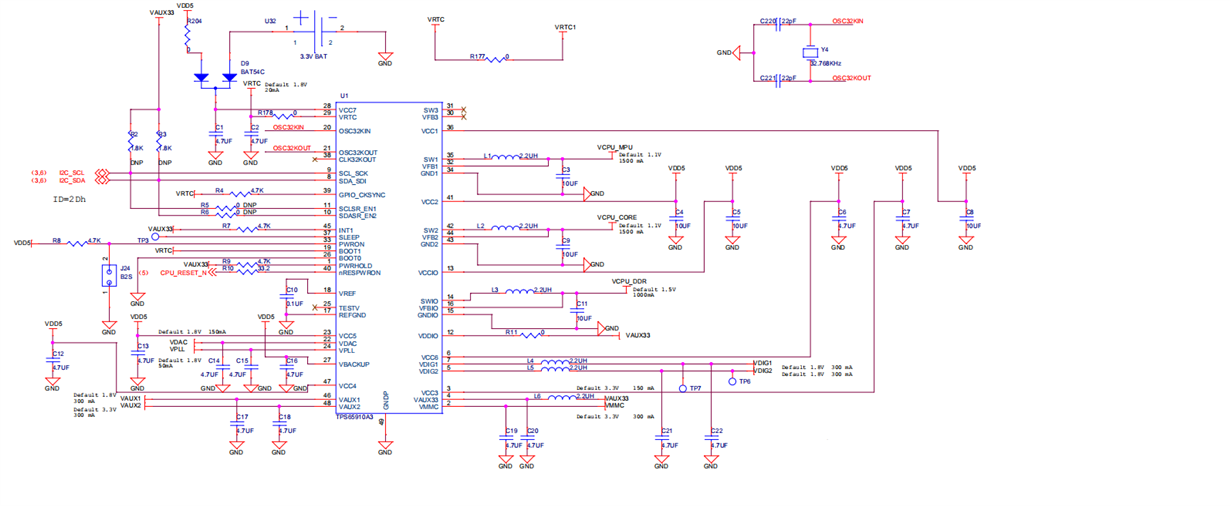
After power up and push the control PWRON to low and then release, no outpu on SW1 or SW2. Other DCDC and LDO is fine. Do you know what's the reason?

Test Result:

Voltage TestPoint Result(V)
VRTC C2 1.8
VDAC C14 1.8
VPLL C15 1.8
VAUX1 C17 1.8
VAUX2 C18 3.3
VCPU_MPU L1 0
VCPU_CORE L2 1.1
VCPU_DDR L3 0
VDIG1 TP7 1.8
VDIG2 TP6 1.8
VAUX33 TP3 3.32
VMMC C19 3.33

  • I noticed that VDD3 is completely missing (SW3 and FB3 pins floating) from your design.

    Is there a reference design that says this wiring is allowable?

    In all the documentation (TPS65910 datasheet, Data Manual for AM335x, etc) it shows VDD3 is wired even when it is un-used. In the schematic checklist, it says FB3 should be connected to GND when un-used.

    If this does not fix your issue, I would look for an accidental short on the PCB from SW1 to GND and from SW2 to GND. This is the only other possibility I can think for the problem you describe.
  • Hi Brian.

    Thanks for your fast comments.

    I just referred the AM3358 EVM schematic and connect VDD3 only. But I think it has no relationship with other DCDCs. Do you think so?

    I have checked the SW1 and SW2 which are not connect to GND.

    I am so confused why no output only on SW1 and SW2. It's quite strange.  I have tested 2 boards and got the  same result.

    Mike

  • Mike,

    According to the schematic checklist, you need to connect FB3 to GND in addition to connecting VCC3 to VCCs (VDD5 on your schematic). SW3 is the only pin that should be floating.

    After reviewing the schematic in more details: I see a few issues that might be causing problems with the design:
    VDIG1, VDIG2, and VAUX33 are all LDOs; therefore, they do not require inductors. L4, L5, and L6 should be removed from your schematic. On your prototype board, you can replace these with 0-Ohm resistors or a jumper wire to connect these power rails to their respective outputs on the board.

    It is possible that the timing of VAUX33 is affected by the inductor (L6), which could prevent VDD1 and VDD2 from powering on.

    Please ensure the rest of your design matches the reference design and the schematic checklist (www.ti.com/.../swca139b.pdf) so that other discrepancies can be identified and removed. I have not reviewed every pin in detail yet, but the issues I have identified must be resolved to continue debugging this issue.
  • Hi Brian

    I removed D9 and short VDD5 to Pin28 directly, it can resolve the issue.
    But I don't know the reason.
    Thanks for your comments. It's also helpful.
  • Not sure why this resolves the issue. The only thing I can think of is that the diode BAT54x has 4 variants.

    It is possible that maybe one of the wrong versions was installed instead of the BAT54C, but I do not see how any of the other version would produce the results you saw unless you are using BAT54S and there is a battery installed but no power applied at VDD5. This still does not seem likely, so it could be a combination of the correct diode and something else that is causing the issue.

    You would need to re-test and measure on an oscilloscope, showing the power-on sequence with D9 installed and without D9 installed. Then I could compare the results and see if anything looks wrong. 

    I still believe wiring VDD3 incorrectly could be related to the issue.