This thread has been locked.

If you have a related question, please click the "Ask a related question" button in the top right corner. The newly created question will be automatically linked to this question.

TPS61021A: Layout for input capacitor and inductor

Part Number: TPS61021A
Other Parts Discussed in Thread: TIDA-00998

Boost team,

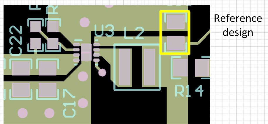
The recommended layout for the TPS61021A places the input capacitor on the far side on the inductor.  Is there a particular reason for this?  If it's possible to place it closer to Vin between the inductor and the Vin pin, would that be better to reduce the distance from the GND and Vin?  

The recommendation is given in the datasheet and I see the same layout is used in TIDA-00998.

Thanks,

Darren

  • HI Darren,

    This cap is to filter the inductor current ripple. So it is better put near the inductor. For the Vin pin decoupling, generally, we'll put another smaller cap, something like 0.1uF near it. But since the total deliver power of TPS61021A is not big, so this small cap can be neglected.

  • Hi Helen,

    Thank you for explaining.  I understand and will recommend this to the customer. 

    I want to put a couple images here to show what I was asking because it might be necessary to change the wording in the datasheet (section 10.1 and section 8.2.2.5).  Or maybe the difference in position wouldn't make any difference with the low currents and a low ESR ceramic cap.  The datasheet states "The input capacitor needs not only to be close to the VIN pin, but also to the PGND pin in order to reduce input supply ripple."

    Thanks for your help.

    Darren

  • Dear Sir,

    I suggest you put the Cin according to the reference design. Because the power consumption on the Vin pin is very small, main power goes through L2.  Move Cin too close to the Vin will cause big noise in the input cable.