This thread has been locked.

If you have a related question, please click the "Ask a related question" button in the top right corner. The newly created question will be automatically linked to this question.

UC3843: UC3843: CC-CV Implementation

Part Number: UC3843
Other Parts Discussed in Thread: LM358

Hi,

I found a 600W Boost converter online. I plan on implementing CC-CV scheme on it to convert it to a Li-ion charger.

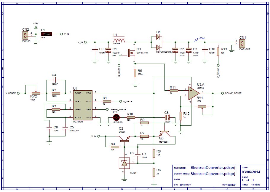
The converter uses UC3843 to generate control signals for the boost FET. I'm attaching a schematic I found of the circuit  its chinese make, so pardon the mistakes)

The converter has two controls - Voltage adjustment and current limiting. The circuit uses LM358. One opamp of 358, U3:A, takes in inductorCurrent sense voltage and generates control signal to limit the inductor current. This signal is sent to ISense pin of 3843. RV1 helps in adjusting the limiting current. Other opamp of 358 is unused. RV2 adjusts the output voltage. A resistor divider is used at the output to sense the output voltage. This signal is sent to Vfb pin of 3843.

So this converter has CV and Current limiting provision. To implement CC functionality, I plan on putting a sense resistor on the output line (low side sensing). The outputCurrent sense voltage will be sent to the 2nd opamp of 358. The amplified signal will be sent to Vfb to control the output such that output current remains constant. Now, there are 2 control signal generation circuits for 3843 (CC and CV). To switch between the two, I'll be using some sort of switch which will be controlled by microcontroller.

My questions are -

Q1. Will this implementation of CC-CV charging work?
Q2. Vfb pin requires 2.5V to operate. What does this mean? How does 3843 regulate the output voltage?
Q3. Is this correct ?  -" Whenever voltage at Isense exceeds 1v, current limiting circuitry kicks in, the duty cycle of FET is reduced to decrease the output voltage and hence the current."

  • Hi,

     I have contacted my colleague to answer your question. He will answer you asap.

  • Hi Pranit,

    First in the attached sch, VFB pin seems not to be connected right, a resister between ground and VFB pin is omitted.
    For Q1, yes this approach can achieve CC-CV charging control, but as you said, a extra circuit or a control method will be needed to switching CV mode and CC mode.
    For Q2, from block diagram in picture in datasheet, we can see that internal reference voltage connecting to non-inverting input of internal error amplifier is 2.5V, VFB pin is inverting input of the error amplifier. So the feedback signal of output voltage connecting VFB pin should be set at 2.5V used for comparing with 2.5V reference voltage.
    The inverting input of internal PWM comparator is a signal proportional to the error amplifier output voltage, the non-inverting input of internal PWM comparator is ISENSE pin, which connects to current sensing resistor and senses the primary-side current. The PWM compares these two signals to terminate the OUTPUT switch conduction to achieve output voltage regulation. The higher VFB pin voltage, the lower error amplifier output, the less PWM turn-time time, lead to lower the output voltage.
    For Q3, yes your understanding is right. The largest voltage value of the inverting input of internal PWM comparator is 1V because of the presence of a 1V Zener diodes, when non-inverting input of internal PWM comparator (that is ISENSE voltage) exceeds 1V, PWM output is terminated.

    Regards,
    Teng

  • Thanks! That cleared my doubts :)