This thread has been locked.

If you have a related question, please click the "Ask a related question" button in the top right corner. The newly created question will be automatically linked to this question.

UCC21710-Q1: UCC21710-Q1:

Part Number: UCC21710-Q1
Other Parts Discussed in Thread: UCC21710, UCC21750,

 Hi,

We want use either UCC21750 or UCC21710-Q1 in 100kW EV battery charger to drive SiC MOSFETs.  We need a peak current requirement of 18A(Both source/sink) with rise and fall times <50ns at switching frequency of 100 kHz.  UCC21750/UCC21710 cannot supply this much peak currents. To accomplish this  task we would like to use external P-channel or N-channel MOSFETs. We need soft turn OFF under MOSFET overcurrents. Please suggest how these ICs can be used to get soft turn OFF feature  when external MOSFET buffer are used for gate driving.

Thanks and Regards,

Raju Baddipadige

  • Hi Raju,

    A BJT buffer can be used with UCC21750 and UCC21710-Q1 to increase the current drive strength to achieve your switching requirements. The STO function can be implemented by adding a capacitor and resistor in series connected to VEE as shown in the image below.

    The capacitor, C_STO, is found based on the equation: C_STO = (I*TOFF)/(VDD-VEE). Where I is the STO current of UCC217xx, TOFF is the desired STO time, and VDD and VEE are the supply voltages. R_STO is present to limit the current during normal turn-off, where R_STO > (VDD-VEE)/10.

    Regards,

    Audrey

  • Hi Audrey,

    We would like to use external MOSFET buffer to meet shorter rise and fall times. We need soft turn off feature during abnormal conditions . Please suggest me how this driver can be used to meet above requirement.
    Please suggest also if any transistors(both PNP and npn) meet these shorter rise and fall durations.

    Raju,
  • Hi Raju,

    We have not performed evaluation of this device using a MOSFET buffer, but I imagine the implementation would be similar to the BJT buffer. However, using the MOSFET buffer will change the polarity of the signal, so you would need to use a logic inverter as well. The rise/fall time of the SiC MOSFET is dependent on the current level, rather than the switching speed of the BJT or MOSFET. The npn and pnp transistors PHPT60410NYX and PHPT60410PYX go up to 20A. We can provide further recommendation with knowledge of your SiC MOSFET. Can you share the part number? Additionally, what are your gate supply voltages, VDD and VEE, and the gate resistance?

    Regards,
    Audrey
  • Dear Audrey,
    Thanks for reply.
    We are using cas300m17bm2,1700V, 300A SiC MOSFET from cree. We have Vdd=20V, Vee=-5V, Rgon=Rgoff=2 ohm. With MOSFET buffer we cannot get soft turn off with this UCC217xx because we need to control gate voltage of N-Channel MOSFET (buffer) to control gate voltage of main Power MOSFET during overcurrents . May be one possible solution is to achieve soft turn off , to have external PNP transistor which connected between gate and Vee with a series resistor. It will be driven by OUTL. During Normal operation power MOSFET will be driven by MOSFET buffer.

    Thanks and Regards,
    Raju
  • Hi Audrey,
    Please also suggest how to bring MOSFET buffer into high impedance when over current is detected.

    Thanks and Regards,
    Raju
  • Hi Raju,

    Thanks for the additional information. As I showed in the circuit above, you can achieve soft turn-off using the R-C circuit and achieve the high current drive you are looking for using the BJT buffer. According to your specifications, you need 20A current drive to achieve 50ns switching of the SiC MOSFET. Based on the drive voltage (+25V, -5V), you should use a maximum gate resistance of 1.1-ohms to achieve 18-A drive. The npn and pnp transistors I mentioned previously are rated for 20A each, so it should provide the current drive capability you are looking for. Please see this e2e post which goes into more detail of the STO design when using a current buffer.

    Regards,

    Audrey

  • Dear Audrey,

    Thanks for the reply. I have few doubts regarding power MOSFET rise and fall times when using below transistors mentioned in the earlier mail

     For NPN BJT,  the specifications of switching transitions  are

    For PNP transistor, the specifications of switching transitions  are

    The rise times for NPN  and PNP transistors are 130ns and 105ns respectively at Ic=5A , Ib=250mA. 

    I have few few queries regarding this,

    1. With these specifications,  can I able to meet power MOSFETs rise and fall times below 50ns.(NPN rise time, 130ns and PNP 105ns)

    2. During turn ON of  power MOSFET, initially difference between gate voltage and driver output voltage will be  higher, transistor base also higher . As the  time progresses the difference between driver output voltage and power MOSFET gate voltage  decreases which decreases base current.    Will decrease in base current of transistor buffer  further increases rise and fall times of Power MOSFET.

    3. The rise times are given at Ic=5A, If we drive these transistors higher Ic(20A) ,  will these further increases rise and fall times of Power MOSFET?

    Thanks and Regards,

    Raju Baddipadige

  • Hi Raju,

    The specifications you inserted are not showing up for me, unfortunately. However, I can still address your questions.

    1. The rise and fall time of the power MOSFET is based on the current drive. The rise/fall times of the NPN/PNP will primarily affect the propagation delay from input to output.

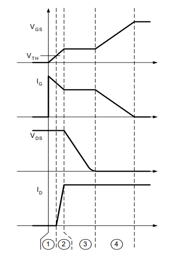
    2. This is normal in driver applications. The purpose of the BJT buffer is to increase the peak current, and in turn increase the current drive throughout the MOSFET’s transition. The peak gate current happens during the transition of the power MOSFET from the low-state to the threshold voltage, after which the gate current decreases, as shown in the ideal turn-on waveforms I attached below. The gate current gradually decreases, as you mentioned, while the voltage increases at the MOSFET’s gate. During the plateau region, the gate current is constant. Once the drive voltage is equal to the VGS, then the gate current is no longer applied. As shown in the image, the voltage and current transition of the MOSFET (i.e. the switching loss) occurs during the 2nd and 3rd intervals. The buffer’s increased drive strength as compared to the gate driver IC alone decreases switching losses by providing a higher drive current throughout.

    For more details take a look at “Fundamentals of MOSFET and IGBT Gate Driver Circuits”. It also has a section on BJT buffer circuits.

    3. It may increase the propagation delay further, but I would need to look into that in more detail.

    Regards,

    Audrey

  • Dear Audrey,

    Thanks for reply. What are the advantages of using MOSFET buffer instead of transistor buffer?. I had an impression that using transistor buffer the following things happens,

    1. we cannot drive power MOSFET gate to power supply rails.
    2. turn ON and turn OFF speed of power MOSFETs is limited due to slow switching transitions of BJT buffer compared to MOSFET buffer.
    3. Typically TURN OFF(tf+td,off) times of BJT are longer compare to TURN ON(tr+td,on) times, there may be shoot through between NPN and PNP transistors which increases the power losses of buffer. This may demand larger power pad /heat sink and higher bias supply power.
    4. Even if we use split output BJT buffer, result will be same as case 3 but less severe.

    Thanks and Regards,
    Raju Baddipadige
  • Hi Raju,

    I took another look at the power device you are driving, and there is an internal gate resistance of 3.7-ohms. Using the recommended drive voltage, you'll only be able to achieve 6.7-A of peak drive strength. Using a buffer circuit will not change this maximum peak current you are able to achieve. UCC21710-Q1 provides higher than 6.7-A (10A), so an external buffer is not necessary.

    Regards,
    Audrey
  • Dear Audrey,

    Thanks for reply and reminding there is a internal gate resistance of 3.4 ohm. A day before yesterday I observed in a failure module that there are 12 chips connected in parallel to meet current requirement and each has 20 ohm gate resistance. It is also there in the data sheet but I did not read thoroughly. But in one application, we need to drive 2 parallel connected SiC MOSFETs(same part number). In this kind of applications, we have solutions with isolator, CPLD(for soft turn off, input signal qualification, under voltage lockout, miller clamp, gate voltage fault, even monitors Vce trajectory during turn on and off, monitors di/dt of device with measuring voltage between auxiliary and power emitter ) on hot side. But this solution is expensive. Please let me know if any future products which have external MOSFET diving and soft turn off feature like ACPL339(This has one problem, it has under voltage lockout on negative power supply which >6.5V. But in my application maximum recommended negative gate voltage is -5V).

    Thanks and Regards,
    Raju Baddipadige
  • Hi Raju,

    Both our UCC217xx family of parts and ISO5x5x parts are isolated with soft turn-off and UVLO. Both devices are compatible to have -5V at the VEE rail. Please take a look at their datasheets and let us know if you have other technical questions about these parts.

    Regards,

    Audrey