This thread has been locked.

If you have a related question, please click the "Ask a related question" button in the top right corner. The newly created question will be automatically linked to this question.

TPS7A4501-SP: ADJ current spec questions

Part Number: TPS7A4501-SP

Hello,

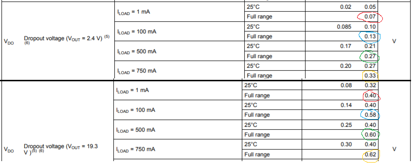
I have a few questions regarding the spec table of this device. Particularly the ADJ pin bias current and the drop out voltage. We noticed that the typical values for ADJ current on page 8 are very different from 25C spec to the full range spec (3uA vs 5.5uA). Also, both these numbers are different than Figure 13 on page 11. Lastly, the difference in drop out voltage between the high and low current parts seemly strangely large. At 1mA and full temp range, the low current part has max 70mV while the low current part has max 400mV.

  1. How is the typical ADJ current measured/defined different when spec-ing the full range number vs the 25C number that results in almost a 2x difference in the numbers?
  2. Is Figure 13 accurate? What conditions is it measured under that could make it so very different from the characteristics table?
  3. Do the two different current variant parts use the same die?
  4. Why are the dropouts for the .75A version so much better?

Thank you!

Regards,
Ryan B.

  • Hey Ryan,

    1/2. These questions are tied together. Figure 13 is accurate and represents a typical device over temperature. The difference between it and the electrical specification is the graph shows a typical device before radiation, life test, and derating due to process variation.

    As far as specifically why the full temp range number is x2 the 25 C number, I think we can agree looking at the graph that the current draw increases with temperature quite a bit. Adding life test which also will increase this number quite a bit and derating, its not unreasonable for the 5.5 uAs to start looking like a more reasonable number

    3. If you notice that different packages for the 0.75 A device vs. the 1.5 A device, there is a thermal pad for one and no thermal pad for the other. This means while the die can handle 1.5 A electrically, whether it can handle it thermally is dependent on the package.

    4. Voltage dropout is caused by the on resistance of the internal FET interacting with the current going through it. Thus if the output current goes up, the current through the FET does as well. I'm slightly confused at your numbers though as the low current part has max 0.33 V drop out and the higher current part has 0.75 max.

    Note package resistance will also effect these numbers.

    Thanks,

    Daniel

  • Hi Daniel,

    Thank you very much for the quick and thorough answers to my questions. I really appreciate the help.

    1-3 are all good on my end, thanks!

    I'm still a little confused on #4, especially since you confirmed that high and low current variants use the same die and just different packaging. The drop out is spec'd at 1mA, 100mA, 500mA, and 750mA. I do notice that output voltage is drastically different, but I'm under the impression the absolute value of the output voltage doesn't impact dropout significantly (please correct me if that's false).

    At 1mA, the difference in maximum drop out is almost 6x! At the higher currents like 750mA, the difference mellows out to a still surprising 2x. Do you mind helping me understand how those numbers could be so different?

    (Top is low current part, bottom is high current part)

    Thank you!

    Regards,
    Ryan B.

  • Hey Ryan,

    Package resistance adds to the FET resistance which causes the drop out.
    Since the devices are in different packages I would expect some difference.

    I believe the typical drop out tells the story.
    The typical number is only 1-10 mVs more than the low current one.
    This makes the most sense if the addition is all package.

    Over full temperature range is where it increases drastically.
    Package resistance of course increases, the larger the package resistance is vs. the FET the more variation that you will see due to changes in the package.

    If I have two numbers like 10 +/- 10% + (1 +/- 10%) I would expect a max range of 8.89 to 11.1 whereas I have 10 +/- 10% + (10 +/- 10%) I expect a range of 8 to 12.

    In short, the package resistance of the larger current device seems larger, which by itself adds some voltage to the total dropout.
    On top of the additional resistance, any variation that was caused by the package is also increased which causes the maximum specs to increase even more on top of that.

    Thanks,
    Daniel