This thread has been locked.

If you have a related question, please click the "Ask a related question" button in the top right corner. The newly created question will be automatically linked to this question.

TPS22975: Large Voltage Drop

Genius 5355 points
Part Number: TPS22975

Hi Support,

Currently our products use TI's Load Switch and DC-DC to implement Power's part.

However, there are problems that find that the voltage drop is very large. Therefore, I would like to ask if the IC solution we choose is suitable and whether there are obvious problems with the circuit diagram design.

The attached part is the circuit diagram of this part.

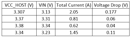
At present, our general situation of Power's Solution is as follows. We find that there is a voltage drop between VCC_3V3_HOST and VIN, and the voltage drop increases as the current rises.

Test data is as follows.

In addition, in the TPS22975 Datasheet, on page 6, it is mentioned that RON at IOUT = -200mA means that if the back load is large, the Load Switch will generate a large voltage drop?

Thanks.

  • Lastly, would like to send schematic offline.
  • Hi Ikon,

    Feel free to send the schematic to me at a-huang@ti.com.

    In general, when we say -200mA, it refers to the current entering the device. Therefore, it simply states that we have a 200mA load on the output of the load switch before measuring the Ron.

    I'm curious to why the voltage drop across the TPS22975 is so large. For example, I'd assume the Ron drop to be ~50mV when running at 2A, not 177mV.

    What level VBIAS as you using? If you're using VBIAS = 3.3V, then the Ron of the device will be larger.

    Thanks,
    Arthur Huang
  • Hi Ikon, 

    I will close this thread sinec we're having a separate discussion over email.

    Thanks,

    Arthur