This thread has been locked.

If you have a related question, please click the "Ask a related question" button in the top right corner. The newly created question will be automatically linked to this question.

LM3488: Rsync On/Off configuration via 3.3V GPIO

Part Number: LM3488
Other Parts Discussed in Thread: CSD19533Q5A, CSD17579Q5A,

Hi, guys. I'm trying to make two custom PCBs with the LM3488MMX/NOPB. Each PCBs will have the MSP432P401R MCU (3.3V).

1) 5V micro-USB powered boost converter to generate 70.40V @ 0.48A

2) Single cell Li-ion 3.7V (550mAh) battery-powered boost converter to generate 70.40V @ 0.48A

With the MPS432, I'm trying to turn on/off the 70V supply which will be connected to a high-voltage Op Amp.

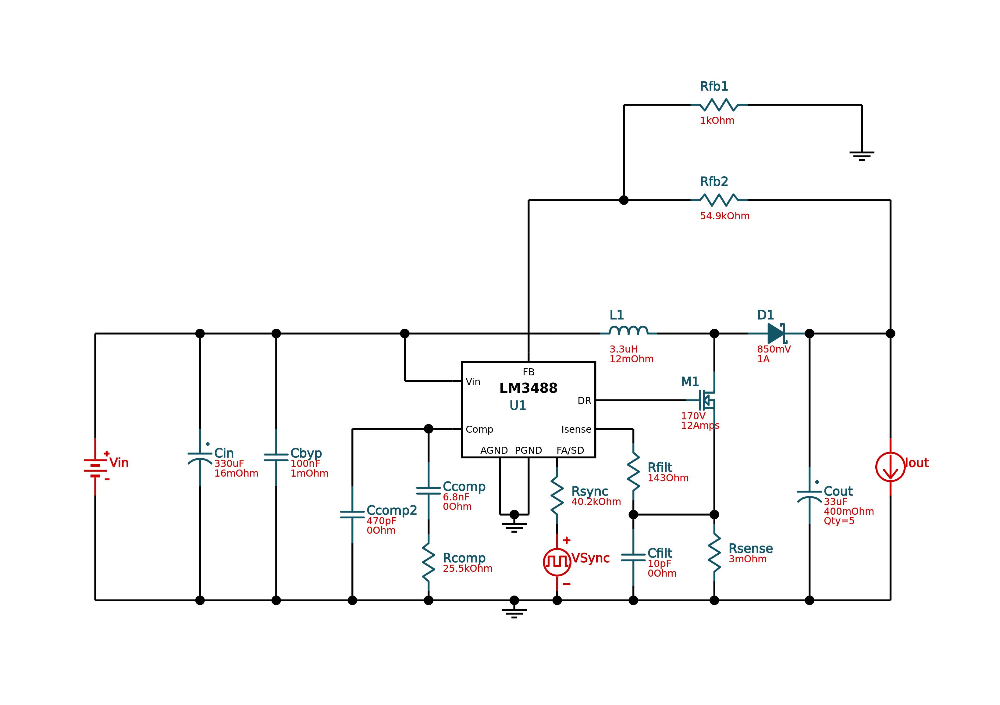
Thanks to the WEBENCH, I got this schematic.

May I ask these questions;

Q0. By using 5V micro-USB or 3.7V 550mAh Li-ion as the input, will this generate the 70.40V output?

From the WEBENCH, it says Vout Actual = 70.43V (I'm fine with the 70.43V), Vout Tolerance = 3.22%

Or will it depend on how I choose M1 NMOS?

Q1. Considering the "M1 IdealFET" specification, is there an NMOS to choose from TI?
Like the CSD19533Q5A (Max Drain-to-Source Voltage = 100V,  Threshold Voltage = 2.8V, Max Continuous Drain Current (Silicon limited) = 75A)?

Q2. This figure demonstrated how to turn on/off the boost converter using the NMOS as a switch

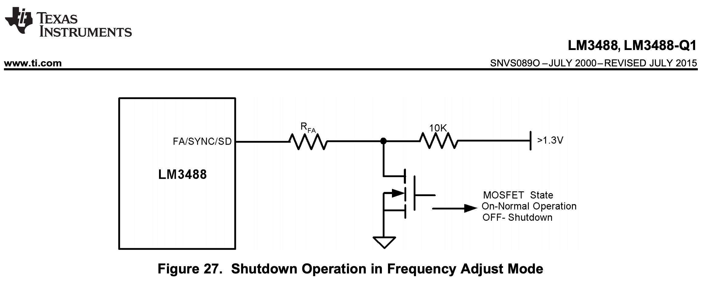
Is it okay to connect MSP432's 3.3V GPIO to the GATE so that I can turn this on/off? I hope CSD17579Q5A (Max Drain-to-Source Voltage = 30V,  Threshold Voltage = 1.5V, Max Continuous Drain Current (Silicon limited) = 46A)can do the job for this.

Also, what value should be the R_FA? I do not have a preferred switching frequency of the boost converter.

  • Hi David,

    Thank you for considering the LM3488. Answers to your questions:

    A0: Yes you can generate 70.4V from 5V input, and it'd better to operate in DCM to avoid running at max duty. However, you may not be able to supply 0.48A. Just do a simple math. For that load at 70.4V, you will need your input to support >6.8Adc, and either your micro USB nor Li-ion battery can support such high current.

    The selection of the FET will affect the max power, and also the efficiency. Datasheet design guidelines address the FET selection.

    A1: Yes you can use the GPIO to control the FET to enable the circuit, but you do not have to use a power MOSFET. This only requires a small signal FET to minimize solution cost, although the CSD1757 can work. RFA is the resistor that sets the switching frequency. Please refer to Figure 4 of the datasheet.

    Thanks,
    Youhao Xi, Applications Engineering
  • Thank you, Youhao. Since you pointed many useful points, let me change this to 70.43V output at 0.3A with 400kHz switching frequency.

    I just chose the frequency after reading this.

    https://www.digikey.com/en/articles/techzone/2015/feb/design-trade-offs-when-selecting-a-high-frequency-switching-regulator

    Youhao Xi said:
    and it'd better to operate in DCM to avoid running at max duty.

    Q0. You are mentioning about the discontinuous conduction mode (DCM), right? Meaning

    "A switch mode power supply enters Discontinuous Conduction Mode when half the inductor current ripple exceeds the average inductor current."

    "During continuous conduction mode, the inductor current in the energy transfer never reaches zero value. In the case of the discontinuous conduction mode, the inductor current falls to zero level which is very common in DC-to-DC converters."

    https://www.ti.com/seclit/ug/slyu036/slyu036.pdf

    https://www.allaboutcircuits.com/technical-articles/discontinuous-conduction-mode-of-simple-converters/

    Q1. May I ask what you meant by "operate in DCM to avoid running at max duty"?

    Q2.

    Youhao Xi said:
    However, you may not be able to supply 0.48A.

    Youhao Xi said:
    For that load at 70.4V, you will need your input to support >6.8Adc, and either your micro USB nor Li-ion battery can support such high current.

    May I ask how did you calculate this "6.8 Adc"?  Also, what do you mean by Adc? Average DC voltage?

    If I modify the circuit to 70.43V output at 0.3A max, I wish to recalculate whether this is feasible with the micro-USB input.

    Q3.

    Youhao Xi said:
    Datasheet design guidelines address the FET selection.

    Thanks, I noticed "8.2.1.2.7 Power MOSFET Selection". Does this mean it is better to have lower

    threshold voltage, On-resistance, Total gate charge, Reverse transfer capacitance, Maximum drain to source voltage?

    Q4.

    Youhao Xi said:
    RFA is the resistor that sets the switching frequency. Please refer to Figure 4 of the datasheet.

    Using "6.6 Electrical Characteristics" table, if I connect RFA = 40k and 10k pull-up resistor, like Figure 27,

    this can be controlled as 400kHz when the MOSFET is on? Or RFA = 40.2k and 10k pull-up resistor which is shown from the schematic?

  • Hi David,

    Answers to your questions:

    A1:  If you just have a few volts Vin and want to boost up to 70V, the duty cycle in CCM can be very large: roughly 94%.  Then the total power will need to be transferred to the load in the remaining time of the cycle, which is only 6%.  You will end up with very high ripple current.  In DCM, the duty cycle can be reduced and avoid such problem.  

    A2:  If you equalize your output power and input power, you will get that current.

    A3: Yes

    A4: When you turn on the FET, FRA will be grounded, and it sets the oscillator frequency.   If you turn off the FET, the pin will be pulled up via the 10k, disabling the IC operation.  I believe the datasheet is clear enough about this. 

    Good luck in your design.


    Thanks,

    Youhao

  • Thanks, Youhao. Two last things, please.

    - You will end up with very high ripple current.

    Q0. WIll adding more output capacitor (ex. 47uF) will reduce the ripple, then? Hope to get some advice, please.

    - In DCM, the duty cycle can be reduced and avoid such problem. 

    Q1. I haven't understood this part; am I able to control the duty cycle of the LM3488MMX/NOPB?

    https://www.ti.com.cn/cn/lit/an/slva061/slva061.pdf

    Also, can I choose this boost converter's mode to be either CCM or DCM?

  • Hi David,

    Yes, you can increase the output capacitor to reduce the ripple voltage. The ripple current is determined by the inductor not the capacitor. 

    You can choose to either operate the part in DCM and CCM by selecting the inductor.   The feedback loop will automatically adjust duty to maintain output regulation.  The article that you referred to in your previous post addresses the selection of inductor for DCM or CCM:  Lmin on page 11.

    Thanks,

    Youhao