This thread has been locked.

If you have a related question, please click the "Ask a related question" button in the top right corner. The newly created question will be automatically linked to this question.

LP8860-Q1: VDDIO/EN unexpected rising before MCU controlling

Part Number: LP8860-Q1

Hi

I found some similar questions in TI community,but still have some question points.

Similar question: e2e.ti.com/.../598729 EN

In our system, MCU uses 5V power supply and LP8860 uses 5V for VDD. SInce LP8860 uses VDDIO/EN as digital reference and VDDIO/EN is input from MCU,we are faced with following condition:

1.MCU GPIO output min=0.7*5V, LP8860 output min=0.7*VDDIO/EN, In worst case the output can down to 0.49*0.5=0.25V which is lower than the MCU H level threshod.

2.We use 5V to pull up LP8860 output:Fault and MISO(SPI communication) to make sure H level can be recognized by MCU

3.According to previous answer: LP8860 has an internal ESD structure forms body diode between FAULT and EN/VDDIO,I guess also between MISO and VDDIO/EN. As a result, when VDD voltage is rising to 5V, VDDIO/EN is also pulled up to a certain value while MCU output still keeps low. And if I cut the connection between MCU and VDDIO/EN, the VDDIO/EN can rise to over 2V which is obviously over the enable threshod.

My question:

1. What's the impact of this unexpected rising? Only make LP8860 enabled before MCU controlling or there's other potiential risk to the whole system?

2. We use 60Hz VSYNC signal as external clock. In datasheet it says VSYNC must be active before VDDIO/EN at power on sequence. But this unexpected rising lead to a result that LP8860 is enabled before the VSYNC. WIll this breake the LP8860 after long time running?

Our original sequence is VDD on-VSYNC on-VDDIO/EN on-Vboost on-SPI to command the PWM on

Now the sequence is VDD and VDDIO/EN on-Vboost on-VSYNC on-SPI to command the PWM on. System can work well after the sequecne and pass power cycle test, but I'm not sure if the change of sequence has bad impact to the product life.

By the way,our VSYNC is generated by LVDS IC and it sometimes will loss due to bad connection with outside loadbox.It cannot always keep active while VDDIO/EN on. That's also a risk or LP8860 just not output PWM without the VSYNC signal?

3.How can we make improvement for our design to decrese the unexpected rising?

Thanks

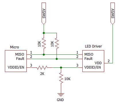
Rough image for our circuit:

  • Hi,

    Please refer to below comments.

    1. What's the impact of this unexpected rising? Only make LP8860 enabled before MCU controlling or there's other potiential risk to the whole system?

    The recommended power up sequence is to enable the device 500us after VDD is active, which can ensure normal power up of the device.

    2. We use 60Hz VSYNC signal as external clock. In datasheet it says VSYNC must be active before VDDIO/EN at power on sequence. But this unexpected rising lead to a result that LP8860 is enabled before the VSYNC. WIll this breake the LP8860 after long time running?

    Our original sequence is VDD on-VSYNC on-VDDIO/EN on-Vboost on-SPI to command the PWM on

    Now the sequence is VDD and VDDIO/EN on-Vboost on-VSYNC on-SPI to command the PWM on. System can work well after the sequecne and pass power cycle test, but I'm not sure if the change of sequence has bad impact to the product life.

    By the way,our VSYNC is generated by LVDS IC and it sometimes will loss due to bad connection with outside loadbox.It cannot always keep active while VDDIO/EN on. That's also a risk or LP8860 just not output PWM without the VSYNC signal?

    I'll need to check the details with the team and come back to you later.

    3.How can we make improvement for our design to decrese the unexpected rising?

    We recommend to pull up the FAULT pin to VDDIO/EN, not VDD. In this way, the unexpected rising can be avoided.

  • HI Shirley

    Thanks for your feedback,hope to get answer of the second question.

    Regarding the third question, we scarcely use one MUC output pin to pull up another input pin for some concern of current consumption and uncertain status during power up.

    Is there other mass product use this kind of design in vehicle  electronics?

  • Hi Shirley

    Is there any progress for my question?

    Thanks

  • Hi,

    It's required that VSYNC signal is active before VDDIO/EN. The main oscillator is enabled after VDDIO/EN is high. if VSYNC is active after that, there will be a uncertain period before VSYNC is active, and the PLL will need some time to settle. We don't think it will break the device. It's just the sequence is not good for stable operation. And the VSYNC must always be active whenever VDDIO/EN is high. Once the VSYNC is lost, the output status can't be guaranteed.

    Regarding the third question, using GPIO from MCU (usually can provide few mA) should allow enough current to use VDDIO/EN supply and pull-down current for Fault pin.

    Fault pin pull-down current will depend on resistor used. Let's assume VDDIO 3.3V, if 10k is used then only  0.3mA will be require for pull down pin which MCU GPIO should be able to provide. For no fault condition, FAULT pin is open/floating and just pull-up high to VDDIO/EN voltage.

  • HI

    Thanks for your reply,I got the answer.

    Some additional question for item1:

    ①Is there any delay between VDD and VDDIO/EN if I pull up the Fault with VDD?Since recommanded sequence is only >500us, current design maybe OK.

    ②ThresholdIf of VDDIO/EN is MIn 1.65V according to datasheet but voltage measured on VDDIO/EN pin is below 1V. Can this ensure the LED driver under disabled status?

    ③How can I measure and judge when the LED driver is enabled accurately? Boost voltage seems to have some delay.

  • Hi,

    Regarding your questions above,

    1. Since there's a diode directly from FAULT pin to VDDIO/EN, the delay will be quite short, much less than 500us.

    2. The VDDIO/EN input low level is 0.4V. The input high level is 1.2V. Only when the voltage is below 0.4V, it can ensure a logic low. If the voltage is between 0.4V and 1.2V, the status is uncertain.

    3. The startup behavior follows the state machine. After the device is enabled, it will first enter the soft start state. After that, it will enter the boost start state, during which the boost can start working. Please refer to the typical start-up waveform in Figure 43 in the datasheet.