This thread has been locked.

If you have a related question, please click the "Ask a related question" button in the top right corner. The newly created question will be automatically linked to this question.

UCC28950: Current sense pin input characteristic

Part Number: UCC28950
Other Parts Discussed in Thread: UCC2895

In my phase shift full bridge converter design I have designed in an RC filter on the current sense input to the chip as recommended in numerous app notes etc, but I am seeing a volt-drop across this filter when I connect it to the current sense input to the chip, as if the chip is loading the circuit. In fact, based on the volt-drop, I would estimate the effective input impedance of the chip to be around 1k ohm. What is more, this impedance seems to be switched as the peak current point is approached, as if a sample and hold is being switched in, which pretty much shorts my current sense signal out altogether, just at that moment.

There is no mention of this kind of behaviour in any literature, so I assumed by lack of any special detail that the input impedance of the pin should be very high. I've seen this with two chips, so I don't think it is to do with chip damage, but I can't rule it out.

Has anyone seen this behaviour before? Is it the expected behaviour?

  • Hello Kevin

    From your description I think that this is expected behaviour although you are correct that this behaviour is not explained in the data sheet. The DS for the earlier UCC2895 device does show this pull down function.

    The input impedance to the CS pin is high during the initial part of the switching cycle. At some point the internal PWM comparator then trips to terminate the active part of the cycle. When that happens an internal 200 Ohm switch is turned on. Propagation delays between the PWM comparator tripping and the current in the power stage being interrupted may make it appear that the internal 200 Ohm pull down activates before the CS signal reaches its maximum but this event happens only after the PWM comparator has decided to terminate the present switching cycle and so it doesn't 'upset' the logic. The purpose of this switch is to help discharge the voltage on the CS pin filter capacitor prior to the start of the next switching cycle. This action becomes more important as the duty cycle increases and there is less time available before the next switching cycle starts. .

    Please let us know if you have any further questions.

    Regards

    Colin

  • Hi Colin

    I'm slightly comforted by your reply, but I see now that my original post doesn't describe what I'm seeing very well - I see the ~1K impedance all the time and a much lower impedance comes in at the end of the pulse. I couldn't find any reference to this behaviour in the UCC2895 datasheet, but I did notice that the UCC2895 datasheet says the input bias current to the CS pin is 20uA - I'm pretty sure I'm seeing a lot more than that.

    The significance here is that it makes it difficult to know what current is going to cause the current limit operation to activate.

    Regards

    Kevin

  • Hi Kevin

    The first thing I'd say is that the input impedance of this pin is much more than 1k and we have many customers using this part successfully without seeing this behaviour. I don't have an actual number for the input impedance so I'll try to run a check on my EVM here this afternoon and get back to you with what I see.

    Regards

    Colin

  • Hi Kevin

    I don't have a hard number for the input impedance of the CS pin but it's orders of magnitude greater than 1k.

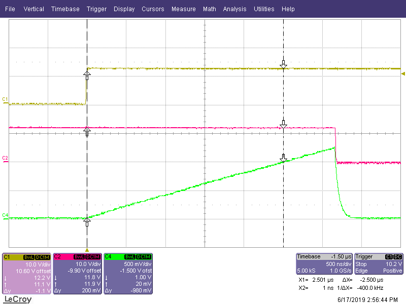
    I connected one of the EVM control boards up to an 'artificial' current sense signal as shown below. This has a source impedance of 130kOhms. You can see that the CS signal increased linearly until the controller PWM comparator terminated it at about 1.25V. Assuming an average 11.5V across 130k gives a current into the capacitor of 88uA. The capacitor is 220pF and the the measured dv/dt of 1V in 2.5us gives a current of 88uA implying that the current into the CS pin itself is much less than this and Rint >>130k.

    I don't know why you are seeing a 1k input impedance - perhaps the CS filter capacitor has gone short or there is some other board fault because the input impedance is much, much higher than that.

    I have only given a sketch of the test method I used here, if you need further details please email me at colingillmor@ti.com and I'll send them to you.

    Yel: OUTA

    Red: OUTD

    GRN: CS

  • Hi Colin

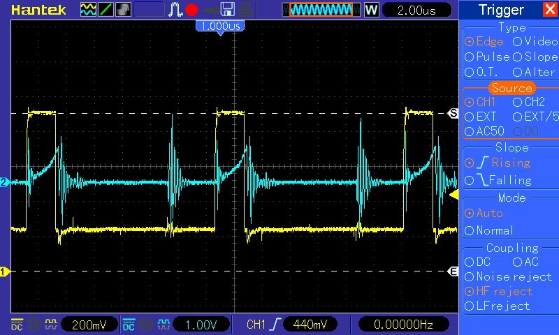
    I have conducted an experiment where I connected the CS pin to a fixed voltage via a known impedance (and no other connections present). The waveform I get when I run the chip like this suggests that the pin is high impedance only during the PWM on-time and is pulled down the rest of the time.

    I must admit, it does look like it comes on and off a bit too early, but for the time being I am satisfied that I understand better whats going on.

    Blue trace is current into the top of the H-Bridge - i.e. PWM current unidirectional. Yellow is the voltage at the CS pin with it connected to a 4K7 / 1K potential divide across the 5V reference.

    Regards

    Kevin

  • Hi Kevin

    What you are seeing looks correct to me - the PWM comparator is tripping on the CS signal plus the slope compensation ramp so that even though the waveform at the CS pin looks rectangular, that at the PWM comparator input will be trapezoidal.

    The reason for the delay between the CS pin being pulled down and the current actually stopping is the propagation delays between the PWM comparator tripping, which is when the CS pin gets pulled down, and the switches in the power stage getting turned off. Of course, once the PWM comparator trips the controller has 'made up its mind' to terminate the cycle and doesn't use the CS signal any more.

    Please let me know if you need any more information


    Regards
    Colin

  • Hi Colin

    Just for clarity, in my experiment, I am using RSum pulled up to force voltage mode and the potential divides that normally hang off the CS signal to set ADelEF and ADel are not fitted. So the ramp to the PWM comparator is not quite as you suggest, but the effect is the same, and your explanation of the propagation delays through my FET drivers etc make sense to me finally.

    Thanks for your help.

    Kevin

  • Hi Kevin

    Thanks for the clarification. Glad I could help and good luck with your project.

    I'm going to close this thread now but don't hesitate to open a new one if you have any further questions.

    Regards

    Colin