This thread has been locked.

If you have a related question, please click the "Ask a related question" button in the top right corner. The newly created question will be automatically linked to this question.

UCC21710-Q1: OC and COM connections with split source Cree SiC MOSFETs

Part Number: UCC21710-Q1
Other Parts Discussed in Thread: UCC21732QDWEVM-025, UCC21750, UCC21732,

Hi,

I am implementing a boost converter using Cree C3M FETs with a split source connection and 2 UCC21710-Q1s for high and low side drive.  I am trying to figure out how to implement the overcurrent protection utilizing the OC pin and a sense resistor I am a little confused on how to connect the source sense pin and source of the FET.  Based on Figure 15 on page 23 of the datasheet it shows a sense resistor (which i have calculated to be 175 ohms to set OC limit to 200A) connected between kelvin source and power source.  Then it shows power source going to COM.  However, everywhere else in the datasheet recommends connecting the kelvin source to COM on the chip and this makes sense as to keep the gate and power loops as separate as possible.  Does using the OC pin prohibit use of the kelvin source on the FET as the COM connection to the chip? Figure 18 shows the same setup but does not explicitly show the connection to COM on the chip (just has a gnd symbol named COM).  Would it not be best to place the sense resistor across kelvin source and source, but still bring kelvin source to the COM?  

I've looked at a few eval boards with similar gate drivers such as CC21732QDWEVM-025, but it only seems to confuse the application more.  For positive OC sensing it shows just a series connection to a 20k (which is a type in the document, the BOM pn shows 2k) and then a filter cap.  For negative OC sensing it shows a 309 ohm shunt resistor across kelvin and  COM which i assume is power source on the FET.  This is confusing since these differences are not explicitly covered in the respective data sheets.  Any guidance on these design challenges would be appreciated.  

-Tim

  • Hi Tim,

    Thanks for posting. Let me first address your questions about the evaluation board:

    UCC21732QDWEVM-025. The 20-kohm (R28) and filter cap (C28) are used for high-frequency noise filtering at the OC pin. The 0-ohm resistors R9 and R27 are there to choose between two methods of over-current/short-circuit protection depending on which version of UCC217xx you are using. R9 is populated if you are using UCC21750, which utilizes DESAT protection for IGBTs. If you are using UCC21732/10-Q1 then you will populate R27 to detect current through a shunt resistor or from a current sense pin of a module. Table 2 of the UCC21732QDWEVM-025 User's Guide gives the differences between the devices and page 22 discusses the configuration of resistors to use DESAT or OC. The configurations for OC assume that there is a shunt resistor external to the EVM or the device/module has integrated current sense, such as the one here

    With regards to the source connection: 

    Figure 15 in the datasheet assumes that the FET shown has integrated current sense pin; this is not the same as the Kelvin connection pin. The IGBT module datasheet I attached previously is a module which has a Kelvin pin AND a current sense pin. For the device you are using, there is not an integrated current sense pin, just a Kelvin source. In this case to use OC detection, you would use an external shunt resistor. The Kelvin source will be connected to COM to minimize gate loop inductance, and you would use the negative current sense configuration to sense across the shunt resistor such that the OC measurement is referenced to COM.

    Please let me know if this answers your questions.

    Regards,

    Audrey

  • Thanks, Audrey.  This makes much more sense now as you pointed out how I was confusing a dedicated sense pin with a simple kelvin connection.  So now how do I calculate the value of my required shunt resistor? 

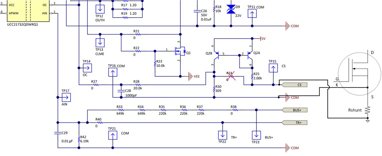
  • Also, just to make sure I have followed you explanation - looking at the Figure 17 schematic for the eval board - I remove R24.  Then I replace the CS pin with a connection to my MOSFETs power source pin and COM is my kelvin source connection.  Is this correct?

  • Hi Tim,

    Correct. You remove R24. Please see the attached image for the connection. Since now you will be sensing negative current, the circuitry with R25, R30 and Q2 acts as a current mirror to translate the negative voltage across Rshunt to a positive voltage. I have derived the calculation, and I believe you will choose Rshunt based on the following:

    Vshunt = I_OC*Rshunt, where I_OC is the current you wish to trip OC.

    We want the voltage across R30, V_R30, to be equal to the OC threshold at the desired current. The voltage threshold to trip OC is 0.7V according to UCC21710-Q1 datasheet.

    The current through R30 is approximately equal to the current through R25. The current through R25 is calculated:

    I_R25 = (5V-(V_shunt)-VBE)/R25 = I_R30

    VBE is approximately 0.7V across the BJT and V_shunt is the voltage measured across Rshunt.

    Using this information, we can find the value of Rshunt to make V_R30 = 0.7V at the desired I_OC using the following equation:

    0.7V = R30*((5V - I_OC*Rshunt - VBE) / R25)

    Then by rearranging this equation, you can find Rshunt given we already know R25, R30, VBE and I_OC (according to your specification, where it is negative given the negative measurement).

    Regards,

    Audrey

  • Thank you very much, Audrey.  This fully answered my question. 

    -Tim