This thread has been locked.

If you have a related question, please click the "Ask a related question" button in the top right corner. The newly created question will be automatically linked to this question.

TPS65218D0: Power down sequence when lost input voltage_2

Part Number: TPS65218D0
Other Parts Discussed in Thread: TPS65218, , BOOSTXL-TPS65218

Hi

This is waveform is power down of AM737xEVM.
Yellow:Input, Green: 1.8V, Blue: 3.3V

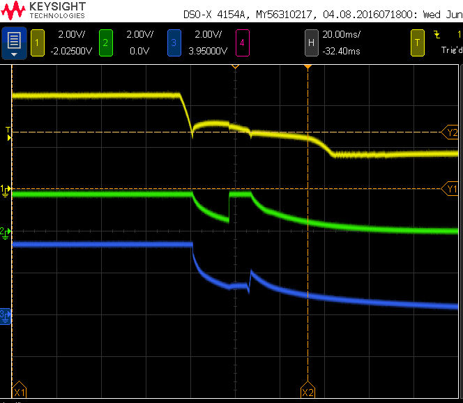
1.8V and 3.3V are power down at the same time.
AM437x datasheet 5.12.1.3 is written as follows;


"If it is desired to ramp down VDDS, VDDS_CLKOUT and VDDSHVx [x=1-11] simultaneously, it should always be ensured that the difference between VDDS, VDDS_CLKOUT and VDDSHVx [x=1-11] during the entire power-down sequence is <2 V. Any violation of this could cause reliability risks for the device."

However, I think that there is not the circuit guaranteeing this issue in TPS65218 or external circuit.
The installation device of EVM is TPS65218B1, will the falling timing be improved in D0?

Please teach me how we should do this circuitry.

Best Regards,
PAN-M

  • Hi PAN-M,

    Your question about the circuitry has been forwarded to responsible applications engineer, however, he will be out of the office and return July 2nd. So answer might delayed a little. Thanks

    Tuomo

  • Thank you for communication
    I wat to solve this problem and want to design in to our customer.

  • PAN-M,

    Please confirm if your question is resolved.

  • No
    A method is not found.

    Best Regards,
    PAN-M

  • For power-down sequence when VIN is lost unexpectedly, I do not expect TPS65218D0 to have dramatically different performance than the TPS65218 (-B1 version).

    The only way I can think of to try to solve your issue is to use the PFI-to-nPFO comparator/buffered I/O feature of the PMIC.

    nPFO will go low when PFI pin falls below 0.8V, and this event can be used to trigger the beginning of the power-down sequence using OFFnPFO bit in the CONTROL register (Reg. 0x06).

    If nPFO is wired to PWR_EN (wire-OR with PMIC_PWR_EN signal from processor) in hardware, this will also trigger the beginning of the power-down sequence.

    This feature is intended to detect an early power failure on the input supply and allow the processor to make a decision to power-down correctly. However, it can also be hard-wired to begin the power-down sequence automatically using the PFI-->nPFO buffer and with nPFO tied to PWR_EN.

  • Thank you for support.

    By see your answer, I understood that there are not measures.
    I think from 50ms to 20ms be necessary in that time when I watch an discharge of each voltage.
    (10 times of 2ms or 10 times of 5ms)
    Therefore I may not be in time for fall time for 5V input of the system even if I use PFI.

    Thanks and Regards,
    PAN-M

  • PAN-M,

    The PFI resistors can be modified as needed to detect the voltage. In the below calculations, I will use the suggested PFI resistors on the TPS65218D0 + AM43xx reference designs.

    VPFI = VIN*R2/(R1+R2); where R1 = 100k, R2 = 22k

    VIN = VPFI*(R1+R2)/R2 = 0.8V*(100k+22k)/22k = 4.436V

    The idea is that when you cross this threshold, the power-down sequence begins and the load decreases incrementally as the power rails turn off.

    Although you do not have 20ms of time in your current scope shot from when VIN starts decreasing to when VIN<2.7V (UVLO), it is possible that you will have enough time as the PMIC sheds the load of each rail during the power-down sequence.

    Does this make sense?

  • Thank you for your suggerst and support.

    There is two power down of DCDC2 and DCDC1 before beginning a power down sequence of 3.3V(DCDC4) of this device.
    During this time, three delays occur, DLY9, DLY8 and DLY7.
    And there are four delays(DLY6+DLY5 and DLY4 and DLY3) before LDO1 off is controlled.
    DLY9=2ms
    DLY8=20ms-50ms
    DLY7=20ms-50ms
    DLY6=2ms
    DLY5=20ms-50ms
    DLY4=2ms
    DLY3=20ms-50ms
    A delay is necessary between 86ms to 206ms, I think.
    This system can not a guarantee to include a delay of VIN from the threshold of the PFI to the threshold of VUVLO over 206ms.
    Because my customer makes only CPU board, not make a power supply.

    I will explain it in reference to your answer to have my customer guarantee the sequence in the whole system.

    Thanks,
    PAN-M

  • PAN-M,

    I do not understand where you are getting 86-206ms from.

    If you refer to SEQ1 and SEQ2 registers in TPS65218D0 datasheet, all delays are 2ms with a global multiplication factor of 1x.

    None of the delays can be 20ms or 50ms if DLYFCTR=0b (1x). They could be 5ms, but all DLY1-DLY9 bits are set to 0b, so the delay is 2ms between each set of STROBE events.

    If you refer to SEQ3, SEQ4, and SEQ6 registers, you will see that:

    • DCDC1 = STROBE8
    • DCDC2 = STROBE9
    • DCDC3 = STROBE5
    • DCDC4 = STROBE7
    • LDO1 = STROBE3

    From PWR_EN low to LDO1 off, there are 7 delays (STROBE10 happens immediately after PWR_EN low is recognized), meaning the total power-down time is approximately 14ms. This is verified by the scope capture below:

    As soon as DCDC1 and DCDC2 power-down, the amount of load on VIN will reduce significantly and the slope of VIN falling will be much less negative after 4ms. If the processor is also responding to the PGOOD low signal, then the power consumption will reduce further.

    Right now, you have 7-10ms from when VIN starts dropping to VIN<2.7V

    Once the power-down sequence begins (by detecting VIN<4.44V), I expect 14ms will be enough time to shutdown correctly before VIN<2.7V

  • Is this waveform AM437xEVM?
    I think that the delay varies according to load capacity when the power off.
    There is no discharge circuit here.
    I estimate this delay to be x10 because I cannot predict this delay.
    Even your waveform thinks that there is 20ms delay, so I think that  DLY1-9 initial setting are problem.
    Is the order of the voltage sequence not be eversed?
    I think that there is a problem when the order of the voltage during the power off is reversed in AM437x.
    Is this correct?
    Do you not have any problem in 2ms?

    DLY3-9 : 2+20+20+2+20+2+20=86ms
    DLY3-9 : 2+50+50+2+50+2+50=206ms

    I informed our customer that it confirm it with an actual system and set a take enough delays.

    Thanks,
    PAN-M

  • PAN-M said:
    Is this waveform AM437xEVM?

    No, this is on the BOOSTXL-TPS65218 programming board with no load on the IC power rails.

    PAN-M said:
    There is no discharge circuit here.

    There is internal discharge resistors in the TPS65218D0 with typical value of 250Ohms for DCDC1-4 and LDO1. If there were no discharge resistors it would take longer to discharge the output capacitors.

    PAN-M said:
    I estimate this delay to be x10 because I cannot predict this delay.

    No, you do not multiply by 10x due to discharging output capacitors. We are talking about the DLY1-9 values when DCDCs & LDO1 begin to turn off. These delays are fixed at 2ms, no multiplier, no waiting for output voltage to reach a threshold.

    PAN-M said:
    Even your waveform thinks that there is 20ms delay, so I think that  DLY1-9 initial setting are problem.

    No, there is no 20ms delay in the waveform I shared.

    PAN-M said:
    Is the order of the voltage sequence not be eversed?

    Yes, the sequence is reversed. Power up is DLY1-9, power-down is DLY9-1. DLY9-3 is shown in waveform I capture.

    PAN-M said:
    I think that there is a problem when the order of the voltage during the power off is reversed in AM437x.
    Is this correct?

    No, the ARM437x works with the TPS65218D0. There is no problem with reverse power-down sequence.

    PAN-M said:
    Do you not have any problem in 2ms?

    No, no problem. From PGOOD low to DCDC2 begin to go low delay is 2ms, between DCDC2 and DCDC1 begin to go low delay is 2ms, and so on. Every delay is exactly 2ms.

    PAN-M said:
    DLY3-9 : 2+20+20+2+20+2+20=86ms
    DLY3-9 : 2+50+50+2+50+2+50=206ms

    No, this is not how to count delays. 50ms would be time from DCDC2 start to go low to when DCDC2 is 0V, assuming DCDC1 waits until DCDC2=0V. This is not the case. DCDC1 begins to turn off (stop switching) 2ms after DCDC2 begins to turn off. The delays DLY1-9 are fixed, they are not relative to the voltage on the DCDCx and LDO1 rails.

  • I was understood that you said.
    However, it is not prescribed timing from the PFI to VUVLO of the customer's system.
    If I get a more detailed customer's situation and  I have some question, I may ask you again.

    Thanks,
    PAN-M