This thread has been locked.

If you have a related question, please click the "Ask a related question" button in the top right corner. The newly created question will be automatically linked to this question.

LM25116: Please help to review the design , used a different inductance and MOS

Part Number: LM25116
Other Parts Discussed in Thread: CSD18563Q5A, , CSD18537NQ5A

Hi Team,

My customer did a design following our  LM25116 Evaluation Board but did some change on BOM.  Their target input,output is almost the same as our EVM, [7-42V input, 5.1V 7A output], I have done the first round check. below is the difference, please help to comment if some potential issue.  thanks.

1. Different divider resistors at FB 【pin 6】,they used 5.1k and 1.6k, but ref design is 3.7k and 1.21k

2. R11 between Vout and VCCX,  does this need or not?

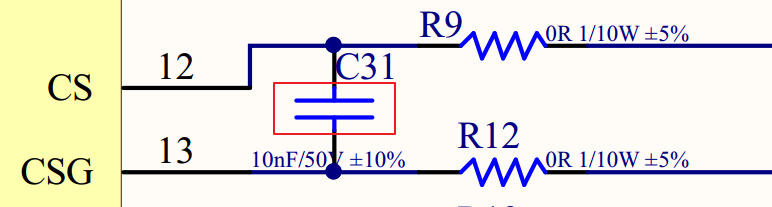
3. An extra capacitor C31 between CS and CSG

4.An extra 0Ω resistor at HO AND LO pin.

5. Different inductance, They used 9,2uH,but ref design is 6uH

6.Different MOS, They used our CSD18537, but ref design is SI7850.

5008.11.pdf

EVM link:

http://www.ti.com/lit/ug/snva232a/snva232a.pdf

  • Hi Yue,

    Here are some comments on the schematic:

    1. No need for HO and LO gate resistors - just use a resistor in series with the boot cap to mange the high-siude FET turn-on.
    2. Consider using CSD18563Q5A for the low-side FET as it has lower Rds-on.
    3. Change boot cap to 100nF - better for startup.
    4. Switch the snubber R and C positions (tie the resistor to GND, better for heatsinking and easier voltage measurement for power loss calculation).
    5. Check compensation values using the LM25116 quickstart calculator (it's available by download from the product folder).

    Regards,

    Tim

  • Tim,

    Thanks for your reply. sorry for the delayed feedback.

    Below is the updated schematic following your suggestion, please kindly double check it ,thanks.

    8540.POWER.pdf 

    A few things may need your confirmation:

    1.  An extra capacitor C31 between CS and CSG

    2.Different inductance, They used 9,2uH,but ref design is 6uH, do you think it would be a problem?

    3. you mentioned " just use a resistor in series with the boot cap to mange the high-siude FET turn-on." , would you please suggest the value of this serial resistor?

    4. The compensation values is the same as our EVM design. since the input, output is the same, can these keep without modification? thanks. 

  • Hi Yue,

    The cap from CS to CSG should be lower value (1nF) and use the R9 and R12 resistors for filtering with a time constant of 10-20ns. The boot resistor can be 5-10 Ohms. Also, you can check the compensation values using the quickstart calculator.

    Finally, note that with VCCX = 5V, there is insufficient gate drive amplitude for the CSD18537NQ5A FETs. See the Qg vs Vgs curve in the datasheet for the Miller plateau voltage (~4.5V) and note that Rdson is specified for Vgs = 6V (not below that). Recommendation is to run from the internal VCC rail of the LM25116.

    Regards,

    Tim

  • One thing is unclear about VCCX.  so , To drive CSD18537, is better to connect VCCX to ground to enable internal VCC rail of LM25116, right?

  • Hi Yue,

    Yes, that's correct.

    Regards,

    Tim

  • Tim,

    Thanks for the reply. below are two option for them, which one do you think is better? this is not their first design. they want to be compatible with their old products .

    1. Changed a MOS which can meet Vgs requirement, keep C30.

    2. Or changed the C30 to a 0Ω resistor to ground

    if 1 is better, can you please recommend a suitable TI MOS? Thanks. 


  • Yue,

    Please consider the CSD18563Q5A 60V NexFET as recommended earlier. Then, you have the option of using the external VCC.

    Regards,

    Tim