This thread has been locked.

If you have a related question, please click the "Ask a related question" button in the top right corner. The newly created question will be automatically linked to this question.

TPS7A4001: Output Voltage drop till 2.5V

Part Number: TPS7A4001
Other Parts Discussed in Thread: LM2936,

In our Application,

Input Voltage = 65V

Output Voltage = 5V

Input Cap= 1uF

Output Cap= 10uF

R1= 100 K (//10nf)

R2= 30K.

we used this device in our Transmitter Product, The RF Output at transmitter port is 30dBm approx,

The device output  Voltage become 3.5-4V (Suppose to be 5V). This cause malfunction in system.

Can you suggest the cause and solution ?

  • HI Himanshu,

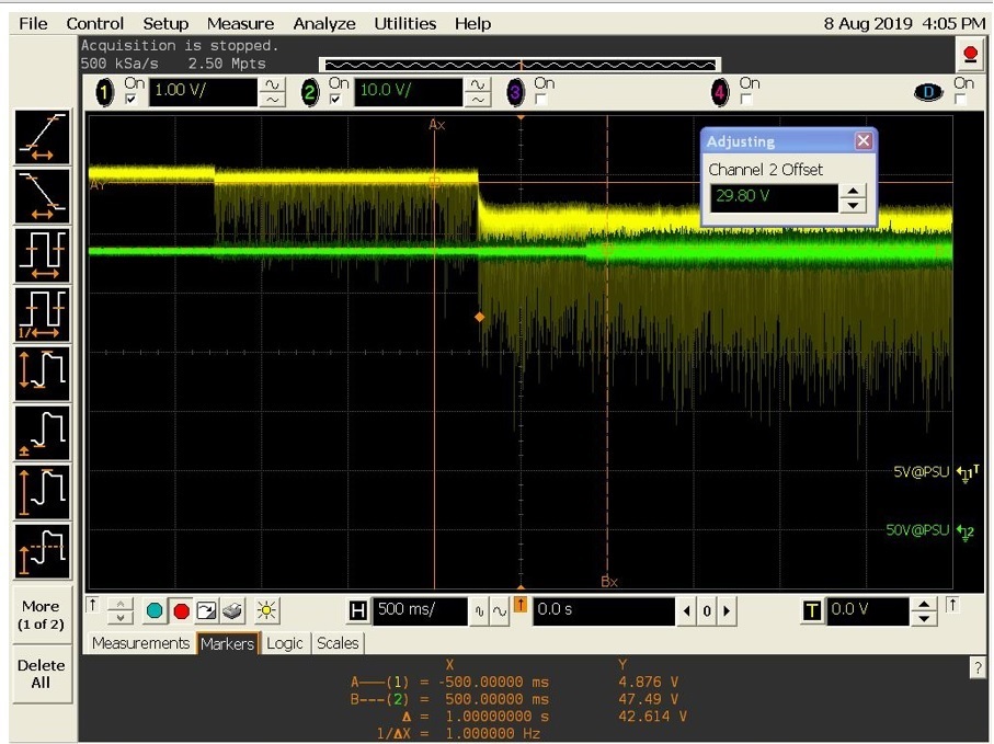
    Can you send scope shots of what is happening? If possible, VIN, VOUT, and IOUT. What is the load current and duration of the transmit pulse?

    I am wondering if you are hitting thermal shutdown.

    Regards,

  • Hi John,

    Load is less than 5 mA. 

    Please Note, The transmitter is not getting power from this device.

    Transmission is continuous.


  • Hi Himanshu,

    With only a 5mA load, from 47.49V to 5V, the LDO is only dissipating ~200mW of power. Normally this would be perfectly fine, but based on the scope shots above, I am wondering if the device is going in and out of thermal shutdown. You would have to zoom in the time scale a lot to see this. Is the thermal pad on the device soldered down properly?

    Can you confirm if the device is getting hot?

    Regards,

  • Hello,

    I have checked with thermal probe, The device is not getting hot. 

    It looks, the device is getting disturbed from RF Output of our transmitter.

    The problem did not occur, When we terminate the RF Output Ports.

    Have you conduct any RF susceptibility kind of test on this device?

    Is it possible the malfunction is due to noise coupled to the device?

    Thanks

    Himanshu 

  • Hello Himanshu,

    It is possible the noise is interfering with the LDO.
    Before we can offer a solution, let's try to pin point the noise mechanism.

    What is your antenna structure during these engineering tests?
    Is it a fixed metalic structure, or more of a loose wire?
    Can you confirm that the antenna is not laying on a conductive ESD mat during testing?
    Can you confirm that the antenna is not a loose wire hanging close by the LDO or electronics (or hovering over the LDO or electronics)?

    Do you have any white wires soldered onto the CCA that could act as antenna's to pick up transmitted RF signals?
    If so, can you be sure the white wires are as short as possible?

    Is there a chassis that the electronics will be housed into?
    If so, is the chassis made out of metal?
    If the chassis is metal, is it possible to find out of the LDO exhibits this behavior when you transmit out of the antenna port and do not terminate the RF?
    This will help understand if the noise mechanism is electromagnetic (far field).

    Please reply back with these answers, and we can continue the troubleshooting.

    Thanks,

    - Stephen

  • Hello Stephen,

    We are using Whip Type antenna for this testing, Antenna is connected on N-type port available at our device.

    antenna is not laying on a conductive ESD mat during testing.

    LDO Electronics is placed on a Board. The board is placed in a metallic Enclosure. (Antenna is placed at outside of metal enclosure.)

    Few connectors ( 2 SMA, one plastic body for power ) are placed at metal Enclosure. 

    Antenna is not a loose wire hanging close by the LDO.

    No hanging wire soldered during testing.

    we observed  malfunction in our system. The LDO must maintain  +5V  to keep the system power ON. And when power failure of our system observed, we probed and  reached at that point, The Voltage drops happen at LDO output.

    It looks, The problem become more worse when we probed the device. But after using a twisted pair cable, routed that cable by a channel ( Not nearby from RF Ports) we could observe a voltage dip on 5V rail. 

    We placed part LM2936HVMAX-5.0/NOPB by rework on board, and the same problem is not observed with this device.

    Can you help me out by this clue?

    Thnaks

    Himanshu

  • Hello Himanshu,

    Thank you for the excellent feedback, this helps a lot.

    My summary of your feedback (please correct me if any of this is wrong):

    1. The electronics (and LDO) are housed in a metal chassis with few holes or slots in the chassis, and the holes/slot are for connectors.
    2. The antenna is a Whip type antenna. During the tests which saw failures on the LDO, the antenna was not hovered over the electronics or laying on a conductive ESD mat.
    3. There are no hanging white wires during test on the PCB.
    4. Twisted pair wires were used to observe the LDO failure while the LDO electronics were housed in the metal chassis.

    Replacing the TPS7A4001 with the LM2936 corrects the issue.

    Next Steps:

    1. I think we should set aside radiated EMI for the moment as our root cause.  This is because of a lack of white wires to couple magnetic field coupling, and the metal shielding should prevent electromagnetic field coupling.

    2. Let's focus on electric field coupling.  Noise can coupling in this way if there is a mutual capacitance between the noise source and the LDO.  Usually this takes the path of parallel planes in the PCB.  Noise on one plane can coupling through mutual capacitance to the adjacent plane.  If you can review your PCB layout, are there any noisy signals directly under the LDO?  Any digital or RF traces, or noisy power signals?  Focus particularly on the area around the FB pin.

    3. How are you wiring in the LM2936? If the LM2936 is not flush with the PCB, or is not in the same location, then this would add evidence to the theory that the noise mechanism is electric field coupling.

    I am looking forward to your reply.

    Thanks,

    - Stephen

  • Hi Stephen,

    you summarised it correctly, I want to add a point, the Connectors are mounted at Panel.

    There is no direct noisy signal set under the LDO area. No other signal present.

    FB pin placed at top layer, ( Layer2 and Layer3 are empty under FB pin) on Bottom layer it is half interact with 5V Out Plane.

    (The board is a 4 Layer Board) 

    LM2936 place at TPS7A4001 location, The connections are done on TPS7A4001 pad by wires.

    The device LM2936 placed die side on board.

    Do you have part TPS7A4001 with Fixed voltage output?

    Thanks

    Himanshu

  • Hello Himanshu,

    I noticed from your first post that you have a 10nF bypass capacitor across R1.  If there is high frequency conducted noise in the system, the 10nF capacitor will look like an AC short and allow that noise to directly couple into the FB pin.  This has been the issue on another post I assisted with recently with this same linear regulator.  Removal of the bypass capacitor fixed the issue for the other customer.  Please remove the bypass capacitor and retest the converter.  If the converter operates correctly, then there is conducted noise in the system flowing back to the LDO output which is coupling through the 10nF capacitor.  You do not need the 10nF capacitor for stability but this does improve AC performance, assuming of course that no noise is coupling through it.

    Let me know the results of this testing.

    Thanks,

    - Stephen

  • Hi Stephen,

    We tried by removing 10nf Cap.

    The results are same as with 10nF Cap was mounted.

    Thanks

    Himanshu

  • Thanks Himanshu, I wanted to rule out the 10nF capacitor.

    I see that there is nothing on layers 2 and 3.  Is there no copper at all?
    Ideally layer 2 would be the return of the linear regulator underneath the regulator circuitry, which would act as an electric field coupling shield.

    On layer 4 underneath the linear regulator, half of the copper is the 5V out?
    Can you offer some screen shots of the layout?

    We may need the placement of the components on the circuit board to help aid in the troubleshooting.
    If you can send that, that would be very helpful.

    Thanks,

    - Stephen

  • Hi Stephen,

    Do you find any solution/workaround for the problem?

    Thanks

    Himanshu

  • Hi Himanshu,

    Thanks, I wanted to rule out the 10nF capacitor.

    I see that there is nothing on layers 2 and 3.  Is there no copper at all?
    Ideally layer 2 would be the return of the linear regulator underneath the regulator circuitry, which would act as an electric field coupling shield.

    On layer 4 underneath the linear regulator, half of the copper is the 5V out?
    Can you offer some screen shots of the layout?

    We may need the placement of the components on the circuit board to help aid in the troubleshooting.
    If you can send that, that would be very helpful.

    Thanks,

    - Stephen

  • Thanks Himanshu.

    Can you confirm what the light blue plane is on layer 3?  I assume it is GND of the TPS7A4001 - is that correct?

    On the bottom layer (blue traces) there is a "12V_EN" trace. 
    Is there a resistor or component which connects the trace "12V_EN" to "VCC_5V"? 
    If so, can we remove this component and see if the TPS7A4001 output voltage issue is corrected?
    I would like to test the theory that the 12V_EN trace is acting like an antenna, picking up noise and disrupting the LDO.

    Thanks,

    - Stephen

  • Hello Himanshu,

    Since it has been 2 weeks, I assume you have been able to resolve your concern.

    If you need any further assistance please let us know.

    Thanks,

    - Stephen