


Hello,
We are using the LM5017 flybuck isolated supply reference design in document SNVR323 http://www.ti.com/lit/df/snvr323/snvr323.pdf
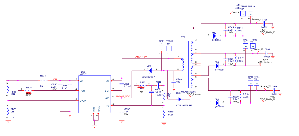
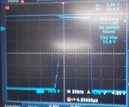
VIN is 48V and I am seeing the SW pin go all the way up to ~58V - what could be causing this? Waveform of SW pin wrt GND:

Waveform of SW wrt VIN (gnd of scope probe connected to VIN) showing a max of 10.8V between VSW and VIN during ON period.
We have measured f_sw and T_on to be correct, but Vout is ~2V higher than what the feedback resistors are calculated to output. Rfdb1 and Rfdb2 are selected for a ~10.2V output but it generally reads ~12V.
I don't think we are overloading the output as the load current never exceeds ~40mA or so, and we have simulated the circuit and do not see this phenomenon.
Oscilloscope and probe have been checked to be accurate as well.
I am wondering if this could be related to the failure where a hole burns in the VIN pin of the chip. Some previous posts here:
https://e2e.ti.com/support/power-management/f/196/t/782471
https://e2e.ti.com/support/power-management/f/196/t/273008
Thanks,
Vishaal

