This thread has been locked.

If you have a related question, please click the "Ask a related question" button in the top right corner. The newly created question will be automatically linked to this question.

TPS63050: TPS63050YFFR land pattern layout information

Part Number: TPS63050

Hi Sir,

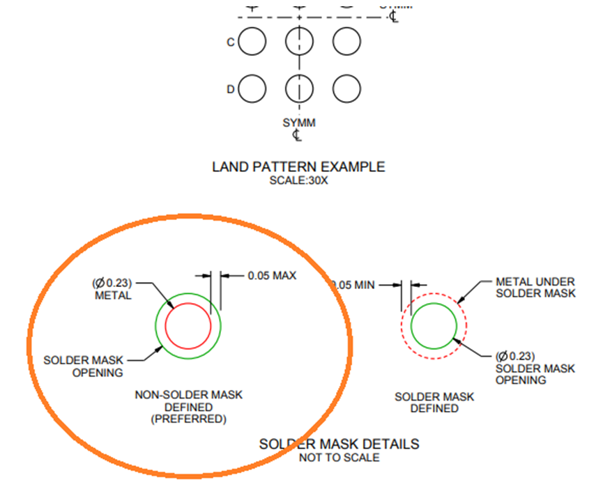
Could you help provide land pattern layout information?

I search in TI web:

http://www.ti.com/lit/ml/mxbg163b/mxbg163b.pdf 

but don't show "D" & "E" value.

In the meanwhile, TI website show DSBGA(12pin)’s length is 2.0mm, but TPS63050YFFR  data show the body size 1.56*1.16mm.

Please confirm the package size of DSBGA(12pin).

Regards,

Driscoll

  • Hi Driscol,

    The same package name may have different D and E dimensions, this depends on the device die size. The correct D and E dimensions are always given in the datasheet.

    The mechanical data page is missing in the TPS63050 datasheet, and the size in the front page table is also wrong, we are working on correcting these errors. In the meantime, here it is from the previous datasheet version:

    YFF0012 - TPS63050.pdf


    And here is the previous datasheet version:
    2047.tps63050_old.pdf

    Best regards,
    Milos

  • Hi Sir,

    May I double confirm with you the DS will charge spec to 1.7mm * 1.3mm, right?

    thanks~

    Regards,

    Driscoll

  • Hi Driscoll,

    The (nominal) dimensions are 1.696 mm x 1.286 mm, and this will be corrected in the next datasheet revision.

    Best regards,
    Milos

  • Hi Sir,

    I have another question about solder mask.

    I see two different drawing of solder mask in package drawing.

    What’s the difference? The drawing on the left side is TI recommend?

    Regards,

    Driscoll

  • Hi Driscoll:

    Really an interesting question. As far as I know, the left drawing is designed for non-solder mask, while the right one is designed for solder mask.

    Please allow me to check the team with deep reason why preferred the left. Thanks for your patient waiting.

  • Hi Driscoll:

    Thanks for your patient waiting. There is discussion during the team. And the preliminary conclusion is conflict with datasheet recommended.

    Please check below:

    "At SMD ( solder mask defined pads ) the solder resistant is always exactly the size which the BGA pad should be open, because the solder opening defines the open pad size independent if the pad is connected by a line a polygon or a via. If the pitch is smaller than 0.5mm we recommend to use SMD ( unfortunately this is often not correctly in the datasheet ).
    At NSMD ( non solder mask defined pads ) the size of the landing pads could be slightly different, because there is a clearance between copper and the solder resistant of mostly 1.968mil ( default, which needs to get modified depending of the pitch sometimes ).
    If looking to the NSMD pad then you can see that the metal part would be bigger if the pad is connected be a polygon, because the copper of the polygon will fill the complete opening which is defined by the solder resistant. Different padsizes could makes problems, like crackes in the device later or soldering issues etc.
    If the distance is 0.5mm between 2 pads and landing pads of 300um we didn’t have problems with NSMD which is the standard, but with a smaller pitch < 0.4mm and a pad size of 230um we need to make SMD.
    Or smallest via have 300um pad which we can place in a BGA pad, therefore the landing pads for NSMD would be always bigger for pads which used Vias or polygons connected to them as the other which use a line connection.
    Often we use NSMD but make the clearance of the solder resistant to the copper to zero, so we will get the same like SMD pads, but we need to modify then the device footprint in the PCB.


    The TPS63050YFF have a pitch of 0.4mm and a Padsize of typ. 250um, therefore SMD pads should be normally recommended."

    I will let you know if there is any updated.