This thread has been locked.

If you have a related question, please click the "Ask a related question" button in the top right corner. The newly created question will be automatically linked to this question.

TPS56121: Design is not working!

Part Number: TPS56121
Other Parts Discussed in Thread: TPS56221

Hello everyone,

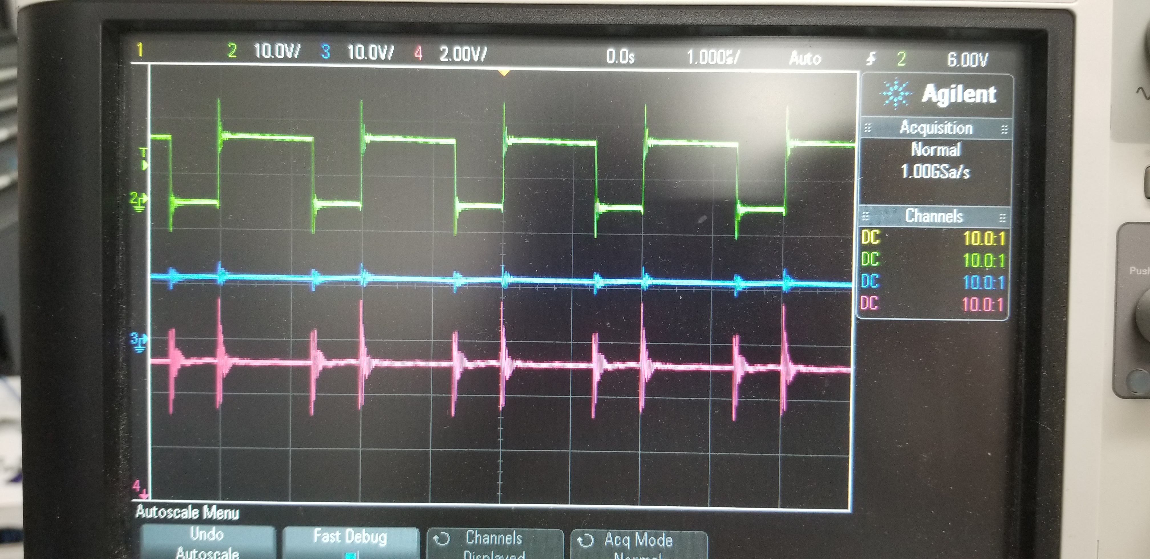
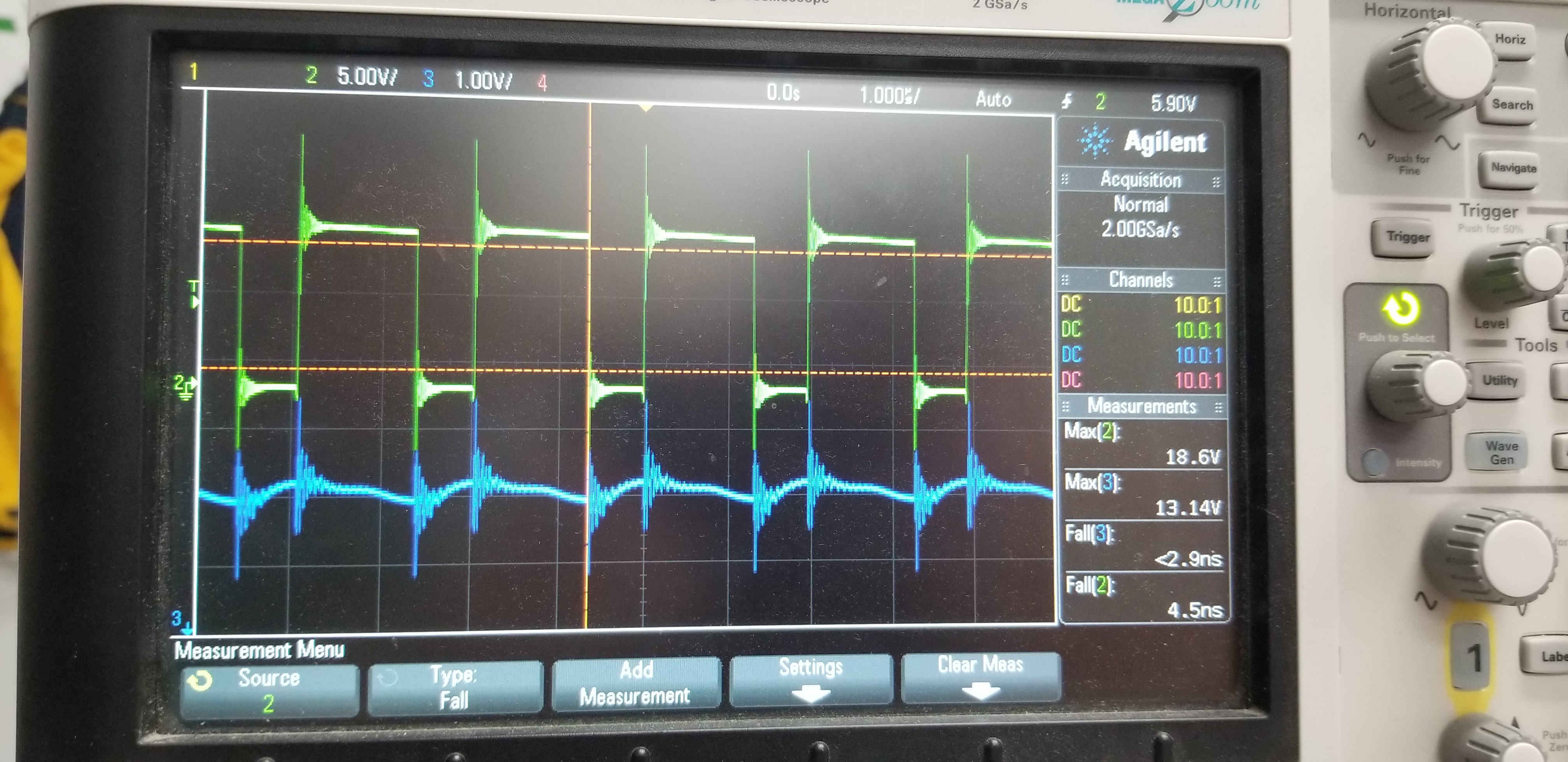
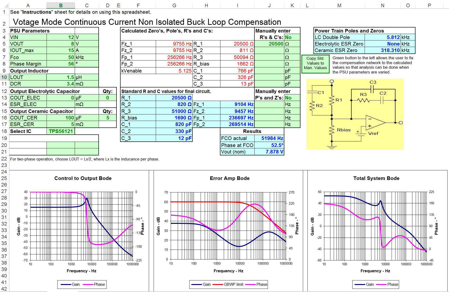
I have designed a 12V to 8V DC-DC converter using spec and circuit layout given for TPS56121. I calculated feedback parameters using Type 3 loop stability excel sheet. Unfortunately, I have no output signal so I can identify where is the problem!?! Any idea?

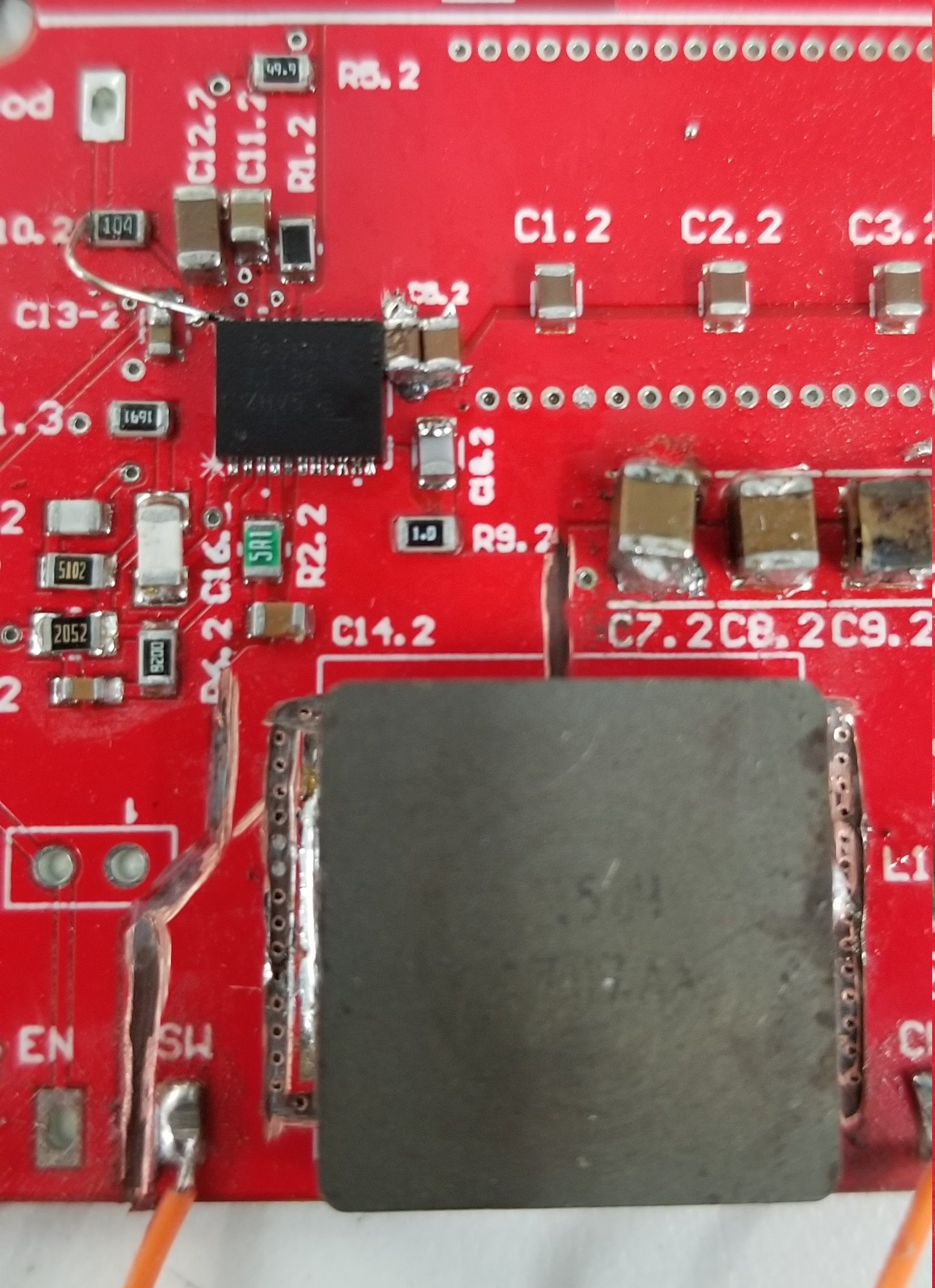
I have attached the circuit layout and schematic is as same as the data sheet. My PCB is 4 layers.

Thanks,

Babak

  • Babak,

    Time to start troubleshooting:

    1. Do you have 12 V at your VIN pins?

    2.  Is EN/SS above the EN threshold?

    3.  Do you have approximately 6.5 V on the BP pin?

    4.  What is the BOOT pin voltage?

    5.  Any switching at all on the SW node?

    6.  Can you capture the start up calibration waveform on EN/SS?

  • Great! Let's start.

    1- Checked. Yes, we have 12V.

    2- EN pin (TP5) have a zero voltage.

    3- BP pin has a zero voltage.

    4- BOOT pin= 0 V

    5-  No switching

    6- No signal. just random noise!

    I think IC is not working!

    Cheers,

  • Babak,

    I suggest you change the IC and try again.

  • Hello again John,

    I couldn't take out the IC so I made a new board. All components are changed except the inductor and capacitor 7 to 10 and C19.

    The results are as follow:

    1- 12V is there.

    2- EN pin (TP5) has a 5.03 voltage.

    3- BP pin has 1.03 voltage.

    4- BOOT pin: 0.58 V

    5-  No signal.

    6- No signal. 

    Cheers,

  • Babak,

    Did EN/SS go thru the calibration sequence at start up?  BP has to be above the UVLO.  Can you send me your Altium project?  j(dash)tucker(at)ti(dot)com.

  • Babak,

    C1.2, C2.2, C3.2 and C4.2 are far away from device VIN and GND pins.

    On the TPS56221 evm the input capacitors are closer to device.

    Can you stack more capacitors on the C5.2, C1.2 or scratch the mask

    to add capacitors closer to the TPS56121 device.

    Place a new IC on board.

    Send an oscilloscope probe of the  VIN and GND voltage.

    Send oscope shot of  BP voltage.

    Send oscope shot of SW pin

  • Thanks for your reply, Davide. Actually, I could figure out what was the problem. The Pgood pin was connected to the wrong side of the R10. After connecting it to another side of R10 everything worked well up to 12A. But I encountered a different problem. For an unknown reason, the current fluctuates after 12A!!!! Any idea why that happened? I captured the SW signal and took a video to have a look.

    I was thinking it is because of the noise. Do you think it is a good idea to separate AGND from PGND and then connect them using a pad?

    This is a picture of gate signal (Green), Output voltage () and Chanel A (red) @ 12A. The behavior of circuit after 12A is shown in the video.

    Video: https://youtu.be/iFuvDGNII5c

    Cheers,

    Babak

  • Babak,

    It could be noise causing the SW jitter since there is a output current dependency. 

    Let us focus on reducing the noise. Use the tip and barrel technique to measurement the voltage in the VIN and GND pins

     Add decoupling and bulk capacitance closer to the VIN and GND pins of the device. 

    Measure the input voltage again.

    David

  • Hello David,

    I made another circuit and by using tip and barrel technique measured the input voltage. Input voltage is definitely messed up!! I also added 47Micro F capacitor (Digikey: 445-1657-1-nd) to the input and measured it again. The noise was reduced but still any value more than 12A circuit had a problem!?! What do you think? I got some pictures for you.

    Gate and input voltage at the no-load condition:

    Gate and input voltage at 12A:

    Gate and input voltage at the 12A with a 47 microfarad capacitor at input:

  • Babak,

    Here are some more suggestions in the attached .    Noise problems are most frequently pcb layout related. 

    See page 21 and 22 of the datasheet  http://www.ti.com/lit/ds/symlink/tps56121.pdf  for additional pcb layout recommendations. 

    4477.TPS56121_e2e.pdf

  • Thanks, David for your suggestions. I did those modifications on PCB (as shown in picture) but the circuit is not working anymore. I may damage the IC, so I need to modify it in the next revision. Before sending the next revision for manufacturing, would you please have a look at it and let me know if a change is required? I have added a reverse polarity circuit to protect the converter.

    I am assuming I should use a different email not John's email. Would you please send me your email address.

    Thanks in advance.

    Babak

  • Please send your file to ddaniels(.dot.)ti(.dot.)com