This thread has been locked.

If you have a related question, please click the "Ask a related question" button in the top right corner. The newly created question will be automatically linked to this question.

TPS61235P: TPS61235P

Part Number: TPS61235P

Hi, 

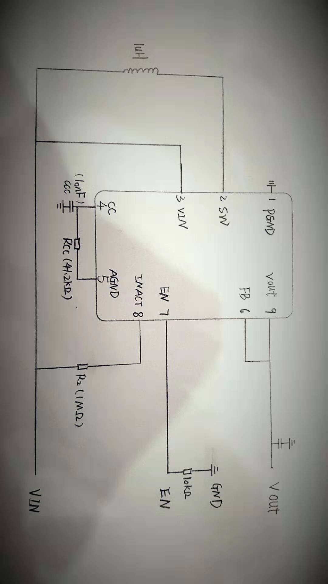
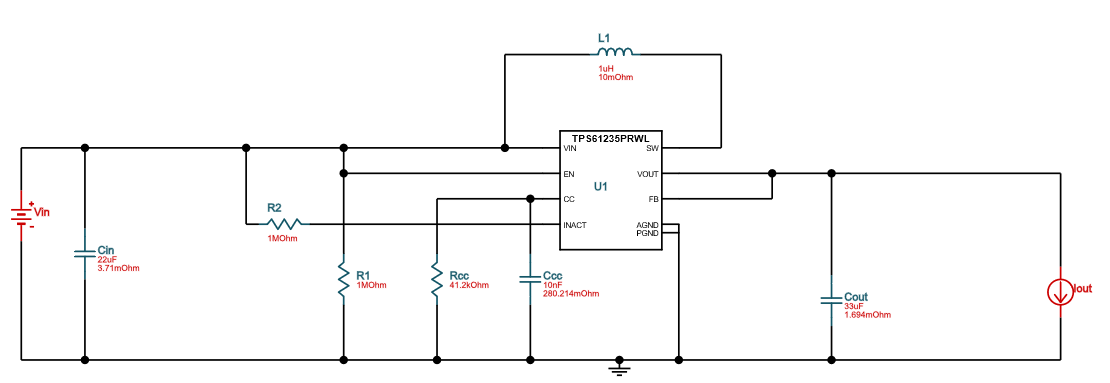
      I  am  designing a  boast  circuit with TPS61235P.  according to Spec, it can get a Fixed 5.1-V Output Voltage, but I get 5.26V without load.

In addition, when I connect a load with 3A discharge , the Output Voltage declines to 4.5V. (Input Source is 4V, 5A).

what is problem with my circuit? 

  • Hi Changgen,

    AGND pin should connect to GND. Input caps are also necessary and should be placed close to device. The required minimum effective input capacitor is 4.7uF. Considering the capacitor's derating under bias, a 10-uF input capacitor is recommended.

  • Hi  Zack:

            Thanks for your help , I have changed input capacitor from 10nF to 10uF, and AGND is connected to GND. 

    It s strange that output voltage is  over  6.0V without load .  at the same time , it can't output  5.1V/3A.  the output voltage is always 4.5V when current is 3A 

  • Hi Changgen,

    Can you share the schematic, layout to me?

    Have you check Vin, SW, Vout, FB waveform? If you did, please also share the screenshot with me. Thanks.

  • Hi  Zack:

         Attachment is schematic  and  layout,  I have not check Vin, SW, Vout, FB waveform. 

    The schematic  is based on "WEBENCH® Power Designer".

  • Hi Changgen,

    I didn't see the layout. Please share the layout.

  • FYI :

                layout :

  • Hi Changgen,

    Are C2, C5, C6 output capacitors? Are C1, C4, C3 input capacitors? Please provide the schematic that has designators so that I could review the layout. The last schematic you shared cannot help me.

    The layout is not good. Input caps and output caps should be placed very close to the IC. C2, C5, C6 negative pad should connect IC gnd pad direclty but now there is very long distance. Parasitic inductance of PCB will cause high spike and ringing during switching and lower the efficiency and even cause instability. Please refer to datasheet page 27 layout guidelines for help.

  • Hi ,Zack:

            Thanks for your help , your suggestion is very useful to me.  my layout is based on last schematic , but is not generated by the circuit.PCB is directly drawn.

     C2, C5, C6  is output capacitors; and  C1, C4, C3 is  input capacitors.  C3,C4,C5,C6 is reserved, does not used . 

            I will refer to datasheet page 27, redraw a   PCB . and test again.  

           Can you give me other suggestions ?  I need 5V/3A output when connected to the load.

    Thanks

  • Hi Changgen,

    You could share the schematic and layout to let me review before sending it for manufacture. 

  • Hi, Zack:

             OK ,  I will share the schematic and layout to you before sending it for manufacture.

    Thanks 

  • Hi, Zack :

            Following is new schemetic and layout, please help me check  them.   the schemetic  is generated by "WEBENCH® Power Designer".  Input  is  a lithium battery , its  output voltage range is 3.3V~4.2V, maximum output current is 9A.  I need  5.1V/3A  fixed output  . (Remarks: R4 can be modified to  41.2KOhm)

          Can I achieve this function?   

    Thanks

  • Hi Changgen,

    It's much better than previous one.

    Why do you put a resistor R2 at output?

    If you don't need constant current feature, R4 could be set to 0 ohm.

    A 1uF input capacitor is suggested at input. Put C3 closer to IC than C2.

  • Hi  Zack:

            I can't  close output   immediately without R2.  If  I pull down EN , the output reduces to 0V  very slowly.

    When I put  R2 at output  and pull down EN , The output voltage soon to 0V. 

           I will modify layout refer to your suggestion.  If there is no problem , I will send it for manufacture. 

     Thanks

  • Hi Changgen,

    OK. Thanks for explaining it.

    There is no problem.

  • Hi , Zack :

             Thanks for your suggestion, we can get 5V/3A output now.  You gave us a lot of help.

    But we encouter another problem:  

            After we close TPS61235P module, wait for a while, then open TPS61235P module , 

    connect a load, enable TPS61235P output.  TPS61235P outputs 25V voltage in a moment.

    and we find  the voltage at either side of  L1  is unusual  after TPS61235P module closed.  the voltage can jump . 

            Why TPS61235P module outputs 25V ?How to reslove this problem? 


     Best Regards

  • Hi Changgen,

    Can you describe the behaviors in more details? How do you close TPS61235p and open it? Did you use a jumper at P1 to enable/disable the device?

    Do you have digital oscilloscope? It will help me a lot if you can show me the startup/ shutdown waveform? Capture Vin, SW, Vout pin waveform if possible.

    When running this test, is there any load connected?

  • Hi , Zack:

            Refer to frames as follows, We open the terminal by  Key, and enable TPS61235P by  EN  pin. 

    then connect iOS phone or pad.  the VCC of USB typeC  can output  25V,  digital oscilloscope can capture it by auto test.

    ATS software can capture it too.  the 25V is short-lived, digital oscilloscope  can't capture pulse waveform. 

           The 25V is not displayed when terminal  works normal.   Pressing Key for a while can switch off power  and close terminal/TPS61235P.

    If we open terminal and enable TPS61235P output , connect load again , the 25V  is displayed.


     Best Regards

  • Hi Zack:

             The   test method about  unusual voltage  may be error ,  we can capture unusual voltage at input side. 

    we should test it by other methods.

            Thanks for your help again .

    Best and regards

    Jerry