This thread has been locked.

If you have a related question, please click the "Ask a related question" button in the top right corner. The newly created question will be automatically linked to this question.

CSD19506KTT: TIDA-00377 Simulation for Solid State Relay

Part Number: CSD19506KTT
Other Parts Discussed in Thread: TIDA-00377, , TINA-TI, TIDA-00751

Dear Team

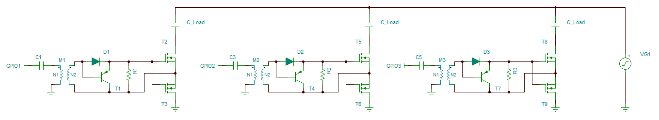
http://www.ti.com/lit/df/tidrjj8/tidrjj8.pdf

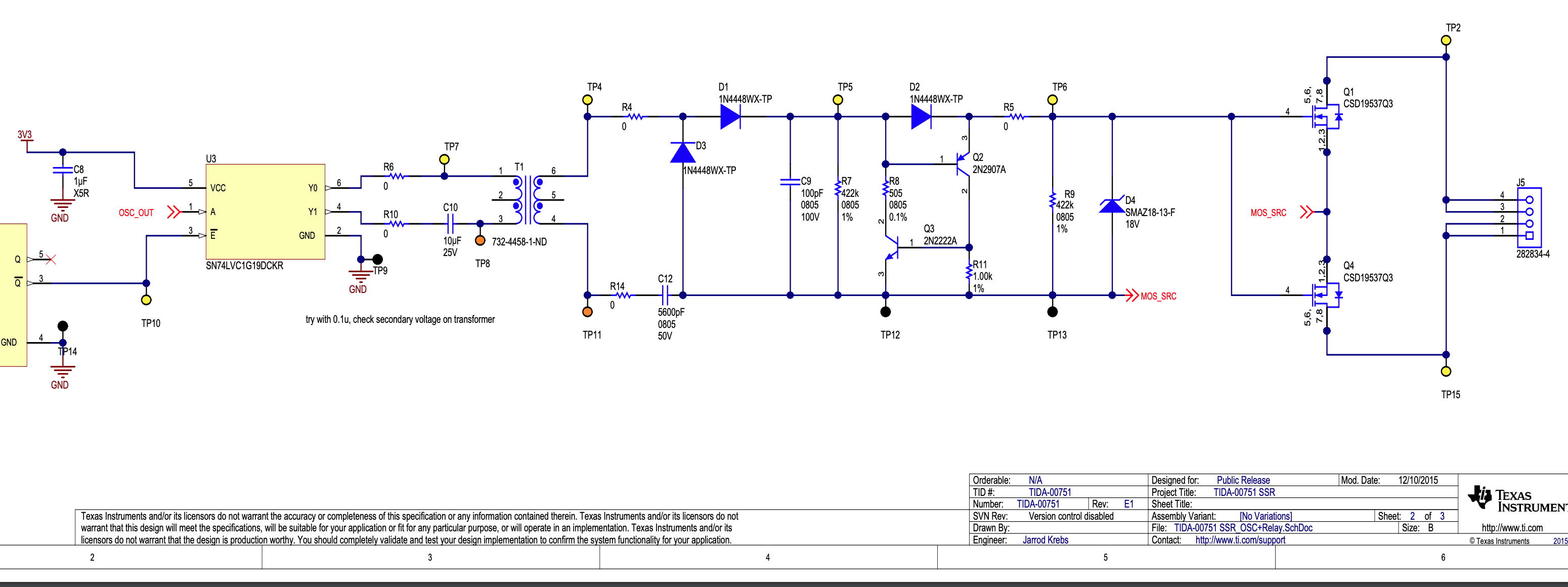
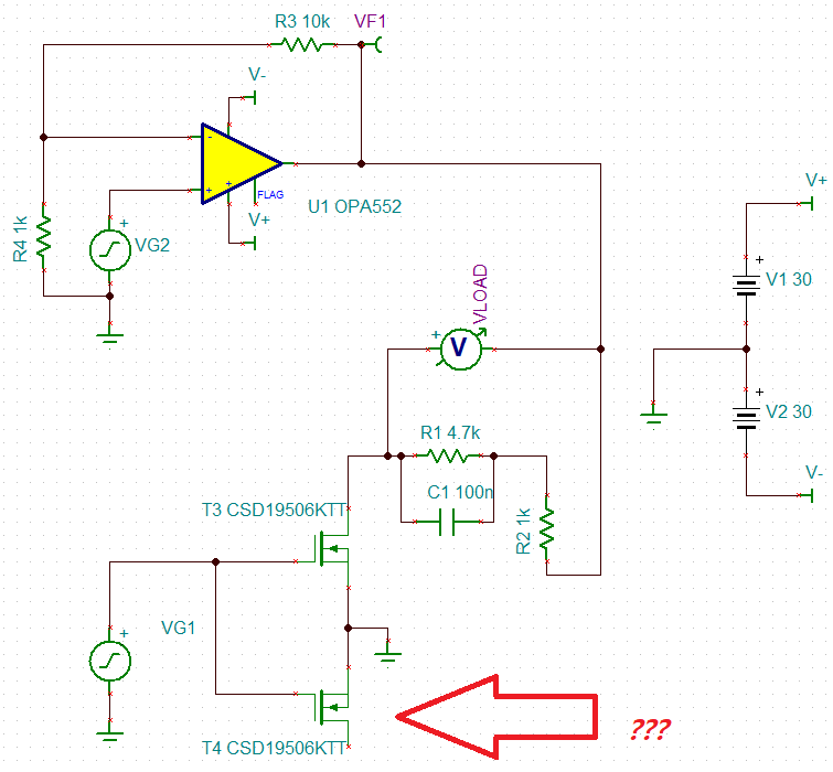
I was trying the TIDA-00377 Solid State Relay SSR using TI TINA 9. I have a custom capacitive load and a sine wave function generator (±30V, 2kHz).

My plan was using an Arduino Uno's 5V GPIO to toggle the NFET.

Since I couldn't find the CSD19506KTT from TINA, I chose a general NFET 2N6755 for the simulation.

From this article,

https://e2e.ti.com/blogs_/b/industrial_strength/archive/2016/07/26/a-modern-approach-to-solid-state-relay-design

I was expecting the AC signal to be flowing through the NFETs when the gate voltage is high.

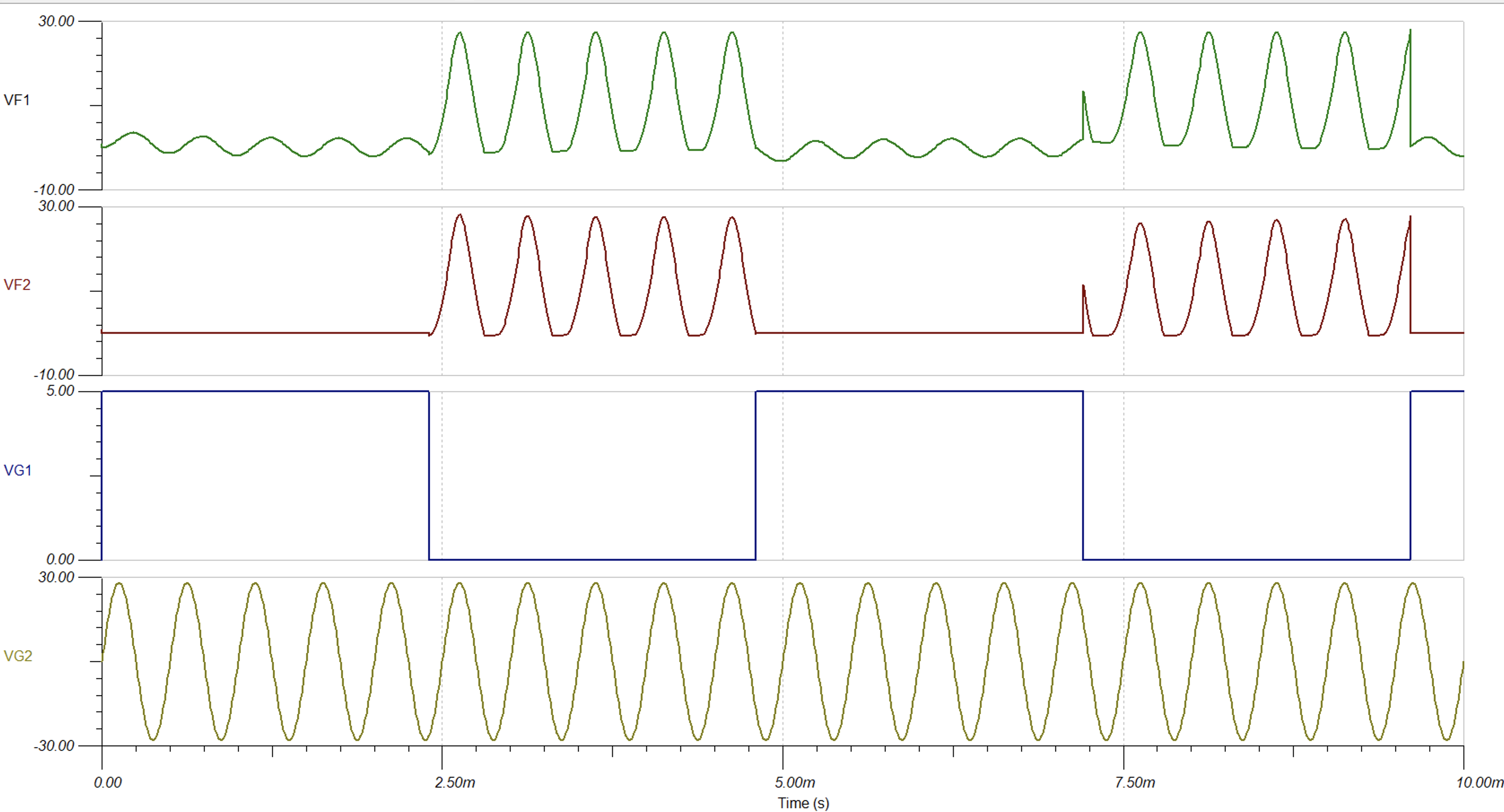
Whereas my simulation result seems like the function generator signal is connected when the gate voltage is 0V, the same GND level from the Arduino board. May I ask

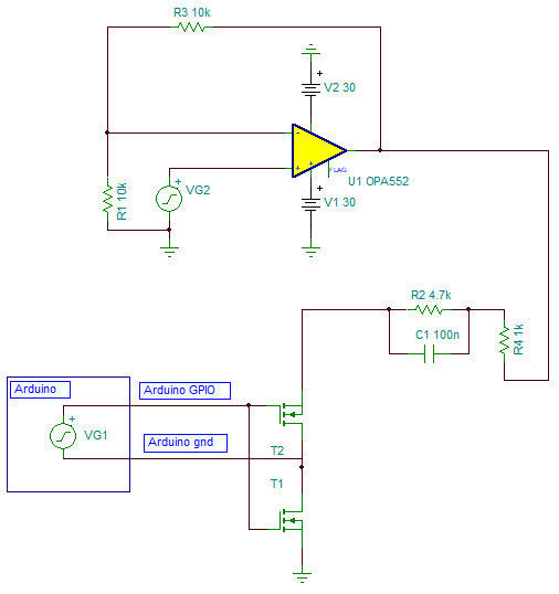
Q0. Is my schematic correct? I thought I followed the TIDA-00377 correctly.

Q1. How can I import the CSD19506KTT into TINA 9? I want to simulate using my desired MOSFET if possible.

Q2. From the outputs (VF1 & VF2), I wanted the VF2 to be 0V when the SSR is off. However, negative voltages are shown.

How can I make this 0V? Should I add a pull-down resistor?

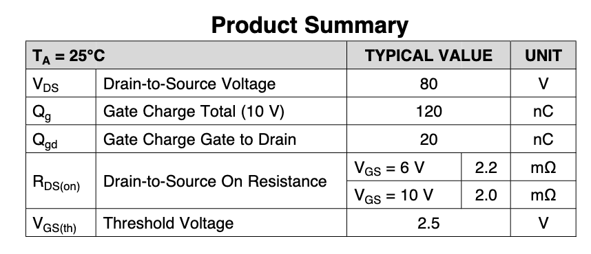
Q3. Using 5V to toggle the gate, can CSD19506KTT be used for the SSR application?

Q4. Compared to the schematic, I need to connect the function generator's negative terminal (-) to Arduino's GND.

Whereas the above schematic has separated the negative terminal from GND.

How should I change the schematic to connect both the negative terminal to GND?

  • Hi David,

    Nice to hear from you again. Let me first start with the TINA-TI model. TI does not publish or post unencrypted models on on ti.com or public forums such as e2e. I am going to send you a friend request and after you accept it, I can send you the unencrypted CSD19506KTT model in a private message. You can then import it into TINA-TI for your simulation. The link below is for an app note that will instruct you how to import a Spice based model into TINA-TI.

    I'm going to have to spend some time looking at your schematic to make sure I understand what you're trying to achieve. I may also ask Miro for his input as he is more familiar with the SSR design than I am. Please note, the CSD19506KTT has rds(on) specified at a minimum VGS = 6V. We cannot guarantee rds(on) at VGS = 5V. Please review the rds(on) vs. VGS curve on page 1 of the datasheet. You can see that VGS = 5V is right at the knee of the curve. This is for a typical device. A slight shift in VTH can cause a rds(on) to increase very rapidly due to the nearly vertical slope of the curve. I would recommend driving the gate of the FET to at least 6V (or more).

  • Thanks, John

    John Wallace1 said:
    Please note, the CSD19506KTT has rds(on) specified at a minimum VGS = 6V. We cannot guarantee rds(on) at VGS = 5V. Please review the rds(on) vs. VGS curve on page 1 of the datasheet. You can see that VGS = 5V is right at the knee of the curve.

    I understand your point. However,

    I saw the threshold voltage is 2.5V. Is this table misleading? Although I saw the graph, I thought 5V could be enough.

    John Wallace1 said:
    I'm going to have to spend some time looking at your schematic to make sure I understand what you're trying to achieve.

    I wish to achieve an application that

    can switch on/off my AC signal to a certain load using a microcontroller.

  • Hi David,

    Please refer to the electrical characteristics table in the datasheet. The threshold voltage is specified at ID = 250uA. The on resistance is specified at VGS = 6V and VGS = 10V. As previously stated, we cannot guarantee rds(on) with VGS < 6V. The device is tested at those conditions during production. I sent you the unencrypted model in a private message. If you can, please put your TINA-TI simulation file into a zip file and send to me in a private message. I would like to run the simulation and see how it behaves. Hopefully, I can figure out the problem.

  • David,

    The simulation looks like it works as intended. The load is in series with the AC source. I added a voltmeter across the R1/C1 and slowed down the gate drive by changing the on/off times to 24ms. When the gate is driven high, the FETs are on there is an AC voltage applied across the load and when they're off the voltage across the load goes to 0V. I'll send you the modified file after I replace the FETs with the TI parts.

  • Thanks for your help, John.

    About Q4;

    "Compared to the schematic, I need to connect the function generator's negative terminal (-) to Arduino's GND.

    Whereas the above schematic has separated the negative terminal from GND.

    How should I change the schematic to connect both the negative terminal to GND?"

    For instance, suppose I have an Op Amp that generates high voltage signal.

    After creating this signal, I want this signal to go through the node when both NFETs are on.

    However, I'm having a hard time connecting the bottom part of the NFET.

    May I ask for help to fill the rest of the part, please?

  • Hi David,

    I am going to forward this onto the Industrial Systems engineer for his help.

  • Thanks, John. Appreciate your help. I'll be waiting for your reply.

  • Your opamp U1 will create sine wave refer to gnd. So you need to have something like this

    That means that your control signal is not connected to gnd but floating

    Hope this helps

    Miro

  • Thanks, Miro. May I ask more detail about this? I'm using an Arduino Uno where its GPIO goes to 5V to 0V.

    - I was using a Non-inverting amplifier to create a AC signal. Do you mean I have to make a open loop circuit?

    I wish to see how to connect this.

    - Is the VG1 the control signal, in my case the Arduino GPIO? Is this separating the GND between Arduino and the N channel MOSFET's GND?

  • Hi Dave,

    From previous post you can see that SSR gnd is not the same gnd of your power circuit. Arduino has different gnd than power portion.

  • Thanks for your kind reply Miro.

    My current problem is that the above signal VGS 2 is created by the Arduino.

    So currently, VGS 2 is using the same ground with the Arduino. In this case, how should I change this?

  • In that case you will need galvanic isolation between VG1 and VG2 as shown in TIDA-00751.

    May I ask you what are you trying to do, for example what is application, system requirements...

    Regards

    Miro

  • Miro Oljaca79 said:
    In that case you will need galvanic isolation between VG1 and VG2 as shown in TIDA-00751.

    Thanks

    I have Op Amps, which will amplify square waves to -30V to 30V, connected to multiple capacitive loads.

    I only want to connect the load to the Op Amp when the Op Amp input gets the input.

    In conclusion, connect the amplified square wave to the transformer and separate GNDs using the transformer, right?

  • Hi David,

    are you trying to do something like this?

    Regards

    Miro

  • Hi, Miro. Yes, something like that.

    One problem will be where is NMOS's source is connected to? To the same Arduino's GND?

    Since you left it floating, I'm curious whether this still needs a transformer/galvanic isolation or not.

  • Hi David,

    this will be an example of the connection. Every single SSR will need to be isolated from Arduino's GND.

    Here I am using three signal transformers to isolate three SSRs. Arduino is controlling three GPIO. Now you will be able to independently turn on and off every single captive load.

    Regrads

    Miro

  • I deeply appreciate your help! One last question before closing this, I believe you need an AC signal from GPIO1 to turn on the transformer.

    Or is it fine to toggle GPIO 5V/0V to GPIO1?

  • Hi David,

    Depends how long you are looking to have MOSFETs on. I will use square wave signal, probably something like describe in TIDA-00377. Your GPIO will go between 0 and 5V with predetermine frequency.

    In addition I will suggest you open separate tread and check stability of the opamp driving captive loads.

    If you need some additional information please do not hesitate to contact me.

    Regards

    Miro