This thread has been locked.

If you have a related question, please click the "Ask a related question" button in the top right corner. The newly created question will be automatically linked to this question.

CSD87350Q5D: CSD87350Q5D Turn on delay time Range

Part Number: CSD87350Q5D
Other Parts Discussed in Thread: TPS51120,

Hi team,

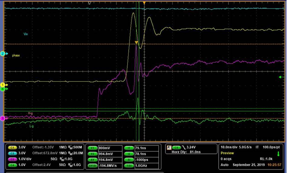
Our customer is using CSD87350Q5D with TPS51120, and when they add a 11A load to the output, there will be a surge at both H/L Vgs, which may cause the H/L FET turning on simultaneously, the surge duration is about 1ns, please refer to the waveform below.

According to the datasheet, the turn on delay time of CSD87350Q5D is 7ns(Q1) and 8ns(Q2), but both is type value, do we have the minimum value? Will the 1ns surge cause both H/L FET on and bring damage to the circuit? Could you please give some comments on that?

Thanks.

Best Regards,

Livia Liu 

  • Hi Livia,

    Thanks for promoting FETs at your customer. It is very common to see a voltage spike on the low side VGS when the high side FET turns on. This is known as CdV/dt induced voltage. The fast changing switch node voltage when the high side FET turns on is capacitively coupled thru the drain-source capacitance of the low side FET on to its gate-sourcd capacitance. I cannot tell from these waveforms if both FETs are turning on at the same time. I would need to see VDS of the low side (switch node) along with the input voltage (AC coupled and zoomed in to see any spikes). The FETs used in the CSD87350Q5D are optimized to prevent CdV/dt induced turn on.The charge ratio of Qgd/Qgs < 1 which minimizes the induced voltage on the low side FET when the high side FET turns on. Measuring the switching waveforms, VGS and VDS, need to be made carefully with a minimal loop between the probe tip and its ground connection. Using the pigtail ground for the scope probe will result in erroneous measurements which show a higher voltage.

    The switching times specified in the datasheet are not very useful as detailed in the link to the blog below. These times are highly dependent on the circuit layout and gate driver used to drive the FET. In addition, I would like to review the schematic if possible.

    e2e.ti.com/.../understanding-mosfet-data-sheets-part-5-switching-parameters

  • Hi Livia,

    Following up to see if this answered your questions. Please let me know. If I don't hear back from you in the next day, I will assume that your questions have been adequately answered and close this thread.

  • Hi John,

    Thanks for the quick support here.

    I just get the waveform you need from our customer, please refer to the picture below(phase=VDS).

    For the schematic, I'll send it to you through email.

    Thanks again.

    Best Regards,

    Livia Liu

  • Hi Livia,

    I am going to close this thread. Please feel free to contact me via email if any other questions come up.

  • Hi John,

    Sure.

    Thanks for your quick support.

    Best Regards,

    Livia Liu