This thread has been locked.

If you have a related question, please click the "Ask a related question" button in the top right corner. The newly created question will be automatically linked to this question.

CSD17575Q3: SON3X3 package footprints

Part Number: CSD17575Q3
Other Parts Discussed in Thread: CSD17304Q3,

Comparing two part datasheets (CSD17575Q3 and CSD17304Q3) with identical packages (SON 3.3mmx3.3mm), looking at recommended footprints:

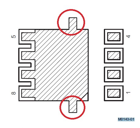
1) Recommended Footprint Drawing note M0143-01 for CSD17304Q3 shows a standard QFN footprint -- along with what looks like a stencil / solderpaste drawing showing with two side "wings" coming from the main pad in the center of the package (is this to deposit paste over the soldermask of the first drawing?)

2) CSD17575Q3  shows a more standard QFN package with a "recommended stencil drawing" that does not show these side "wings"

What is the recommended footprint for this "Q3" package?  Is there a reason that these two tabs are not included in all "recommended footprint" drawings for this package?

Thanks - James

  • Hi James,

    Thanks for your interest in TI FETs. I've got an inquiry into my SMT experts to answer your questions. The CSD17304Q3 datasheet is older than the CSD17575Q3 and the information may have changed but the datasheet not updated. I will send you a more detailed response as soon as I have more information.

  • Hi James,

    I have confirmed with my SMT expert that the information in the CSD17304Q3 datasheet is outdated. The shaded area represents the component footprint. The larger area without color is the PCB pad. The datasheet did not provide any stencil information. We plan to update this datasheet but it may take a little while to complete. In the meantime, the datasheet of CSD17575Q3 has both PCB land pattern and stencil. These drawings are correct. Please use them for your design.