This thread has been locked.

If you have a related question, please click the "Ask a related question" button in the top right corner. The newly created question will be automatically linked to this question.

TPS2662: Behavior during Start-Up Short-Circuit On Output

Part Number: TPS2662
Other Parts Discussed in Thread: LMZM23600, , LM5180

Hello,

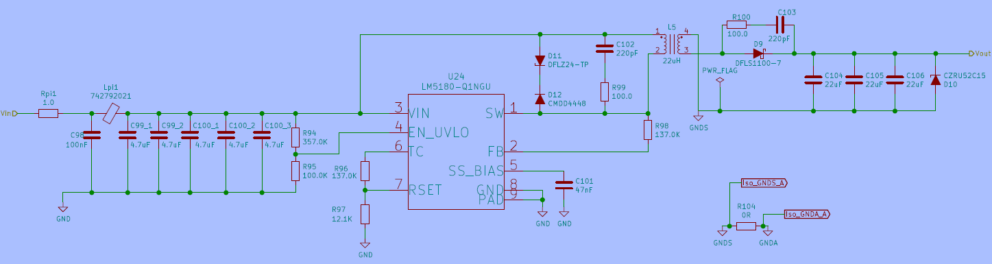
I have a prototype board with that feeds both a Buck module (LMZM23600) and a Flyback (LM5180-Q1NGU). 

For some reason, the output from TPS26624 is behaving as if there is a short-circuit at the output (data listed below). I have the following questions:

  1. Is the data below consistent with short circuit at the output per Figure 40 of the datasheet or is there a possibility that the assembled device defective? 
  2. Could this be related to load characteristics; I attached the schematic of the interfaces between the TPS26624 and the Buck module (LMZM23600) and Flyback (LM5180-Q1NGU). 

DMM Data

Vin = 12.6V (to GND)

RET to GND = 1.995V

 Vout = 1.33V (to GND), 

~FLT = Vout

VR1 = 12.6V (to GND) - OK

VR2 = 3.77V (to GND) - OK

VR1 = 0.376V (to GND) - OK 

I also attached the design data for TPS26624.

Thanks for your help!

Design Input

Parameter Description Value   Units Tolerance
VIN (max) Maximum System Input Voltage 36.0 V  
UVset Undervoltage Lockout Threshold 6.90 V  
OVset Over Voltage Cut-Off Threshold 33.00 V  
Cout Load Capacitance 33.0 µF 10%
TA (max) Maximum Ambient Temperature  TA = 85C °C  
RLstart Load during start-up (Assumed to be resistive) 100.0  
Imax Maximum continuous load current 0.6 A  
ILimit Current Limit, 10% higher than the maximum continuous load current 0.66 A  

R1_cal Calculated value of Resistor at IN pin 681.7 kΩ  
SELECT THE CLOSEST POSSIBLE RESISTANCE VALUE FOR R1, R2, R3        
R3_sel Selected closest possible value for R3 resistor 30.10 kΩ 1.0%
R2_sel Selected closest possible value for R2 resistor 115.00 kΩ 1.0%
R1_sel Selected closest possible value for R1 resistor 698.00 kΩ 1.0%
UV_Final Undervoltage Lockout Threshold 6.99 V 3.4%
OV_Final Over Voltage Cut-Off Threshold 33.70 V 3.4%
Power Fail Detection Power Fail Detection Threshold 6.39 V 3.4%
I_R123 Current in R1, R2, R3 Branch 42.70 uA  

sio_Power_Protections.pdf

sio_LDO_MCU_A.pdf

sio_Flyback_A.pdf

  • Hello Lasto Roma,

    Is the Output of TPS2662 providing power to input of buck (LMZM23600) and Flyback (LM5180)? 

    if yes, it could be due to higher current during startup. You can try below modifications:

    • Increasing current limit of TPS2662 by reducing RILIM
    • Reducing Inrush current by increasing Cdvdt cap of TPS2662
    • Increasing UVLO set-point of LM5180

  • Thank you very much for your reply.

    Yes he Output of TPS2662 providing power to input of buck (LMZM23600) and Flyback (LM5180). I attached an overview document that lists all power devices and rails (all standard power circuits from TI).

    When I disconnect the power to the LMZM23600 modules (D and F in attached document), both the TPS2662 (A)  and the Flyback LM5180 (B) seem to be working fine. I also disconnected LDO LP38798SD-ADJ (C in document).

    I'd appreciate if your team/app engineer could review the overall power supplies diagram in the attached document. All circuits are basic TI design but there seem to be interface/startup/sequencing issues.

    I can send you all TI configuration parameters that were used in TI web designs.

    Best Regards

    Sio_Prototype_Overview.pdfsio_isolated_buck_A.pdfsio_LDOs_Unipolar_A.pdfsio_LDOs_Bipolar_A.pdf

  • I collected some data after I disconnected the Buck circuits and connected TPS2662 output to the flyback LM5180 only, as shown in the diagram below.

    I noticed that the output of the TPS2662, is reduced from 12.6V to 5.75V and it is oscillating (charging and discharging cycles with ppk = 2.16V). What changes should we make to the circuits below to avoid this instability.

    TPS2662  Vin (Vsupply) = 12.6V  

    TPS2662 Vout (Vprotected) = 5.75V average with ppk = 2.16V

    LM5180 Vout (Viso) = 14.9V +/- 3mV  [Per design this should be 13.2V)

    Thanks.

  • Hello Lasto Roma,

    Are you using TPS26624 or TPS26625? Can you please share the waveform for VIN, VOUT, ILIM and FLT pin of TPS2662 with oscillations on output of TPS2662.

    For review of schematic of LMZM23600  and LM5180, please post new queries on e2e for each part with part number in the subject.  

  • Hello Lokesh,

    I'm using TPS26624DRCT. I'll send the waveforms.

    Thank you.

  • Attached are the waveforms for  VIN, VOUT and FLT pin of TPS26624; and Output from the LM5180 (Flyback)

    The signal for ILIM is 1V +/- 200mV (measured across ILIM resistor; i.e., w.r.t. RTN not GND)

    Please let me know if you'd need further information.

    Thanks!

    @ 500 msec/div

    @ 50 msec/div

  • Hello Lasto,

    This could be due to Rpi at input of LM5180 and switching frequency of LM5180. You can try reducing Rpi and increasing cap at input of LM5180.

  • Hello Lokesh,

    I disconnected the  LM5180 circuit from the TPS2662 (removed Rpi) and connected a dummy load across Vout. 

    Below is the snapshot of the output of TPS2662 with and without a dummy load of 200 Ohm (load repeatedly connected and disconnected. There are no oscillation). 

    It seems that one of the fault conditions of TPS2662 is occurring for some reason. According to the datasheet, the fault conditions are undervoltage, overvoltage, over load, reverse current and thermal shutdown. I assume others would assembly issues or defective device.

    Any suggestions on how to isolate the specific issue would be appreciated.

    Please let me know if you'd need further data.

    Thanks very much for your help.

  • I also measured the input current from the supply, while connecting 200 Ohm across TPS2662 output pin 10 and GND, as Isupply =  0.5 mA.

    There is no issue with the Vin=Vsupply supplying proper current (e.g., Isupply = 81 mA if the 200 Ohm is connected on the input side pin 1 to GND, when Vin = 16.2V).

     The input current from the supply, at no load, is Isupply = 44 uA. 

    Please let me know if you'd need further data.

    Thank you.

  • Hello Lasto,

    There is difference of ~2V between IN and OUT of TPS2662. At NO Load, VIN=VOUT for TPS2662. Are these voltages measured at PINs of TPS2662?

    Can you verify the RILIM resistor used for TPS2662? Is it 10k?

  • Hello Lokesh,

    I measured VOUT at the pin and the ~2V still there (same as in the snapshot above). I noticed that when connecting DMM the difference is at 500mV then it starts to leak down to ~2V.

    Here's additional DMM data that might be of interest:

    VIN to GND = 16.69V  [pin 1 to pin 6]

    RTN to GND = 15.82V [pin 5 to pin 6]

    VOUT to RTN = -30.0 mV [pin 10 to pin 5]

    VOUT to GND = 16.1V leaking to 15.6V [pin 10 to pin 6]

    I already verified the value of RLIM directly between the pins (5 & 7) and it is 10K. I also verified values of all other passive  components around TPS2662.

    Please let me know if there are any other measurements that you need.

    Thanks very much for your help

  • Hello Lasto,

    What is the part number of Diodes used for D33 and D34? Can you also share the layout for TPS2662 and its peripheral components?

  • Hello Lokesh,

    Thanks very much for your continued help.

    The TVS diodes D33 and D34 are SMBJ24CA-13-F (Datasheet Link). I also attached the layout (as .pdf and kicad).

    REF PART NUMBER MANUFACTURER BOM DESCRIPTION Footprint
    D33,D34  SMBJ24CA-13-F Diodes Incorporated TVS DIODE 24V 38.9V Bi-Directional SMB Diode_SMD:D_SMB

    Just to make sure that you have all relevant schematics, the interface between external supply BATT and TPS26624 is depicted below. (where VDDF is the same as Vsupply in the TPS26624 schematic sent earlier). 

    Please Let me know if you'd need any further information or data.

    Best regards.

  • Hello Lasto,

    Can you check if RTN (Pin 5) is properly soldered and connected on PCB? 

    Can you check if issue is still there when RTN is shorted to GND externally on the board?

    Please mark TPS26624 in the layout or send the layout of TPS26624 and its compoenets.

  • Hello Lokesh,

    I'll double check continuity of RTN (Pin 5), and reflow if necessary.

    The measurements, listed above in the post, of RTN to GND = 15.82V [pin 5 to pin 6], what value should RTN to GND be/expected in normal condition? Anyway, I'll connect them.

    I included the layout below, I could not attach the layout file itself (file type not permitted on the forum; but I can send it externally directly to you if necessary).

    Thank you!

  • Hello Lokesh,

    I re-checked continuity of Pin 5 per the layout below and it seems to be fine.

    Interestingly, when I connected RTN (pin5) to GND (Pin 6), as you suggested above, the output voltage VOUT and VIN matched (with few 100mV at no load) which seems fine.

    Next, I disconnected RTN from GND and reset TPS26624 using SHUTDOWN (and recycled Vsupply) and everything seems normal afterwards (VOUT=VIN) at NO LOAD.

    I then added dummy load resistance across VOUT and I measured the load current.

    If the load is around 500 Ohm, then VOUT tracks VIN (with IOUT=VOUT/Rload; in this case 40mA at 17V). However, if I change the load to be around 300 Ohm, TPS26624 goes to the shutdown mode (VOUT~200mV), and needed to be reset after removing the load.

    My understanding is that based on the Rlim (10K), the current limit should be 600mA. So, I assume TPS26624 is shutdown for some other reason.

    Thanks for your help.

  • Hello Lasto,

    Thanks for sharing the layout. I could not find anything in the layout which could cause this behavior.

    Can you confirm if you are observing RTN (Pin 5 of TPS2662) voltage as 15.8V more than GND voltage (Pin6 of TPS2662) ? (Pin 5 [RTN] is positive w.r.t Pin 6 [GND])

    On how many boards are you observing this behavior?

    What is the voltage difference between Pin6 (GND) and GND pad of Input caps C143, C151,152,153,155,156?

    What is the voltage difference between Pin6 (GND) and GND pad of Output caps C145,146,147?

  • Hello Lokesh,

    I checked RTN to GND at both no-load and load conditions and the reading I'm getting is +0.6V (Not sure under what condition that I had 15.8V).

    I have only one prototype board, but I can replace the device on that board with a new one if necessary. The TPS26624 is the first circuit on the board and is currently being isolated from everything else.

    I removed the device and tested the passive components on both the input and output sides, to ensure that no current limits from the Vsupply or short-circuited components.

    I place the device again, and it seems to shutdown if the load connected draws more than 50mA (with a spike around 70mA). If the load draws less than 50 mA everything is working fine once I reset the device.

    The device fails to start if there is a load (any load connected during the startup).

    I connected 0.1uF to slow down the dV/dt during startup, still TPS26624 fails to start.

    I'll replace the device and keep you posted.

    Thanks.

  • Hello Lokesh,

    I replaced the TPS26624 device with a new one and it seems everything is normal now (no shutdowns on startup so far, and output voltage values are correct). It seems that the original device became defective somehow.

    I'll perform more tests and let you know if I run into any issues.

    Thanks for your help.