This thread has been locked.

If you have a related question, please click the "Ask a related question" button in the top right corner. The newly created question will be automatically linked to this question.

BQ24192I: Questions about CE pin and the values of switching inductor and output capacitor

Part Number: BQ24192I


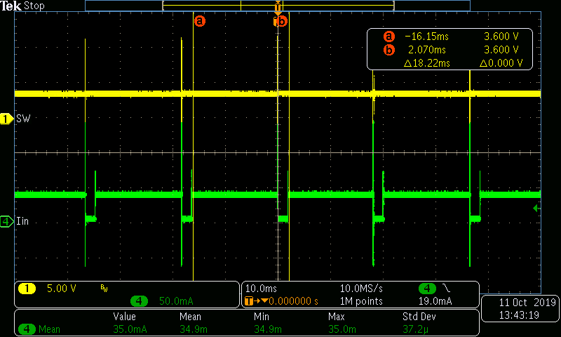
1. Why there is still switching waveform even if  the chip is disabled by pulling /CE pin high?

2. If switching inductor = 1uH, and output capacitor = 10uF, the input current will be around 30mA when the battery is absent.

    if the values are chosen as BQ24192i EVM design(2.2uH and  2*10uF), the input current will be about 2~3mA without battery.

    Why is that?

Thanks very much for your explanation.

  • Hello,

    Regarding 1, /CE is charge disable which only disables charge current flowing from SYS to BAT through the internal battery FET Q4.  The charger's buck converter provides the higher minimum system voltage or battery voltage at SYS unless the HiZ register bit is set to 1 and BATFET disabled bit is set to 1..

    Regarding 2, the inductor current and output voltage ripple will be less with 2.2uH and 2*10uF but I would not expect a 10x difference in input current.  When running without SYS load and no battery, the input current will be pulsing either in DCM or PFM.  It is likely that the input current meter is not measuring correctly with the 1uF and 10uF LC as compared to the 2.2uH and 2*10uF.  The app note below explains the issue related to PFM and how to add an large input capacitor to average out the pulses.

    http://www.ti.com/lit/an/slva236a/slva236a.pdf

    Regards,

    Jeff


  • Jeff,

         I used the same test measuring method for both 1uH+10uF and 2.2uH+20uF.

         Basically, the app note says that, under PFM mode ,an additional capacitor of large value is needed to avoid  AC component so that the current meter in series can read the value accurately.

          I tried with a 2200uF capacitor at the input, the current is still large ,about 30mA.  As I used the current probe to read the current value, I think it can handle the AC component.

         CH1 is SW node, CH2 is the input current read by a current sensing probe.

    Below is the situation when the additional capacitor is removed, almost the same as above


              I also tested the waveform of the inductor current, it is nearly 0mA


    It seems that when the values of inductance and capacitance are not proper, the internal circuits of the charger IC will consume more current. 

     How do you think?

    Best regard,

    Wolf

  • Wolf,

    It appears that you are correct.  The datasheet gives the following guidance for sizing the LC filter:

    To get good loop stability, the resonant frequency of the output inductor and output capacitor should be designed between 15 kHz and 25 kHz. With 2.2-µH inductor, the typical output capacitor value is 20 µF.

    A 1uH and 10uF LC is outside the 1/(2*pi*(LC)^0.5) recommended resonant frequency.

    Regards,

    Jeff

  • Jeff,

         Thanks for the information.

          Yes, I also noticed the description in the datasheet. I just wonder how improper values result in  the abnormal current.

     Wolf.

  • Wolf,

    Most likely, the lower LC combo leads to loop instability and oscillations inside the chip.  Oscillating circuits consume current.

    Regards,

    Jeff