This thread has been locked.

If you have a related question, please click the "Ask a related question" button in the top right corner. The newly created question will be automatically linked to this question.

UCC2897A: UCC2897A secondary phase spike overspec issue.

Part Number: UCC2897A

Dear Sir,

Our customer is using UCC2897A and we have the secondary side phase spike over spec and the spike is reach to 270V(CH2)@1,25A which is too high and over spec (the diode spec is only 200V). please see the waveform as below

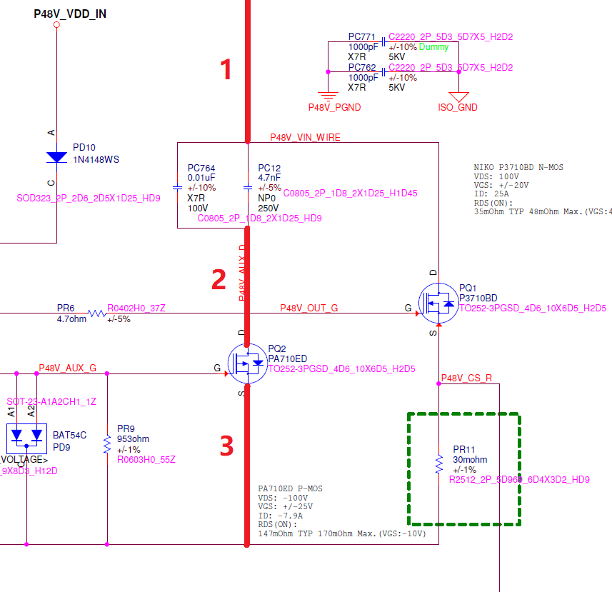
And we try to place snubber on PD12 and PD13. the snubbuer on PD13 have no improve on the spike and the one in the PD12 would improve the spike  but it would have a spike pulse shown in the waveform below and also the waveform which RD can't use the solution. Could you kindly give us some suggestions to improve the spike(RD need to push the spike under 180V). we also attach the schematic as below  

Above,please kindly help us with issue that we have and hope to hear for you soon

Cheers

Alec


  • Hi Alec,

    An expert will get back to you soon. Thanks.

    Teng

  • Dear Teng,

    We have co-worked with RD and currently. out best spike is around 240V with 2.2 mohm and 470 pF(the larger/smaller R don't really help much with spike and the larger capacitance would cause Vout up-normal drop). However, we also found another issue  about adding the sunnber , with any snuuber solutions placed on, there is chance to lose Vout power output after around 1 min with full load(normal again after removing the snubber) . Therefore, it seems that we could have the sunnber on the the diode in order to have the normal power performance. 

    Therefore, please kinldy let us know if there is solution that we could try to solve this spike issue . thanks in advance

    if there is any question ,please feel free to let me know

    Cheers

    Alec

  • Hi Alec,

    I can't open the schematic you attached , could you please send it again ?

    Thanks.

  • Dear

    Here is the schematic as your reference again.Please kindly give us some advise. we have been co-working wiht RD for a week and we still have no suitable soltion for this issue

    4201.SCH.pdf

    if there is any other question, please feel free to let me know

  • Hi Alec,

    Can you capture transformer primary winding current , Main FET Vds and Vds of PD12 in the same waveform when the issue happens?

    Thanks.

  • Dear Jaden,

    Here is the PD12(phase) wavform with sunnber(2.2mohm+1nf )and we have tried 470pf, 680pf, 1nF(R vaule didn't really improvethe spike) and the waveform are all similar expect 1nf have best spike proformace which is 232V. and it still over spec for PD12(200V). Also, with sunnber on , the power would shut downin few mins understand full load. Therefore, RD can't use this a solution for now.

    As the main FET Vds and transformer current wavfrom, we will update to you later, RD's dealine for this issue is 10/15. Therefore, we will need your kind support for this soon as possible. hope to hear form you soon,

    Cheers

    Alec 

  • Dear Jaden,

    Add the main FAT wavform:

    Full load without sunbber:( 1.25A, CH2: Vds)

    Full load with snubber :( 1.25A, CH2: Vds)

    As the transfromer current waveform , we are still working on it and will update to you later, and if there is any solution base on the data that we provided, please kinldy let us know, we coudl verify it wiht RD here.

    if there is any other question, please let us know

    Alec

  • Hi Alec,

    Could you please tell me which point did you captured the Iprimary ?  looks like it's not transformer primary winding current . or the clamping switch is not normally turn on during main switch turn off time. the larger spike on secondary diode was caused by hard switching of main FET.

    Could you please check if clamping switching are normally turn on ?

    thanks

  • Dear Jaden,

    We the the transformer primary winding current on the "A" point shown as below

    And according to you, the spike might be  caused by the main FET swrtching. However, we have tryied to adjust PR6( gate resistor) value. and there is no improovemnt  for both samller value and bigger value. Currently, we still have no suitbale solution got the spike issue. please kinldy let us know if you have any suggestion/solution that we could try here.thanks

    if there is any quesiton, please let us know

    Alec

  • Hi Alec,

    Adjust gate driver resistor value only can speed up/down the turn on slew rate of MOSFET , But what we are talking about are hard switching or ZVS.

    before the main FET turn on , there is must have a negative current through body diode .then the FET can achieve ZVS turn on. you can find it in below image. and compare with the waveform you captured from customer's board . there is no negative current in customer's board .

    so I you have to find out what happens at clamping switching FET.

    In the second image below , point A and point B are different , the current through point A contain both magnetizing and Demag. current .

    but through the current Point B only contain  when main FET turn on.

    I have attached a application note , please forward it to the customer , make sure the customer engineer familiar with some basic knowledge and  debug experience.

    Thanks.4667.Understanding and Designing an Active Clamp Current.pdf

  • Dear Jeden

    Many thanks for the update. We will look into the AUX MOS behivor wiht the negative current to see if our measurement is correct.

    At the other hand, RD's design is based the simulation form the wenbench. And currently RD's desgin work fine expect the spike is over spec. Could you kinldy give us the suggestion for improving the spike besides the snuubers? thanks in advance

    Hope you hear form you soon

    Alec

  • Hi Alec,

    I have proposed my suggestion in previous two posts : Find out why there is not negative current before main FET turn on , check if the Clamping switch FET didn't turn on after main FET turn off . 

    The larger spike was caused by main FET hard switching , because we didn't find the negative current before it turn on in your captured waveform.

    If it still not clear , please feel free to let me know.

    Thanks.

  • Dear Jaden,

    We understand what you said. However, the clamping FET is controlled by UCC2897A and it seems that there is no much that i can adjust.  And the circuit was base on EVM or Webench provided by TI. Could you give us more detail solution that we can try here. This issue have been going on for one month.

    We need your great support to solve this issue as soon as possible.

    We attachment the latest circuit and primary side FET VDS, current waveform as your reference again(the Iprimary is measured at the A point in your previous feedback)

    Cheers

    RD Johnny

    If you need the layout board file to confirm. Please give us your mail address I will pass it for you.UCC2897A_circuit.pdf

  • Hi Johnny,

    I have reviewed your schematic and testing waveform , I have two questions as shown in below:

    1. In the schematic , there is a capacitor PC775 (10nF) parallel on Main FET and current sense resistor. could you please let me know what purpose of this capacitor ?  since it will caused a large discharge current when main FET turn on . and the negative current maybe is not enough for ZVS turn on of main FET due to a lot of energy needed for discharge this capacitor.Can you remove this capacitor and test again?

    2. In the testing waveform . you can find the driver signals for each FET are correct . but when the main FET turn off , primary current reach to peak current.

    then it suddenly drop to below zero and with a large ringing , it should be pass the body diode of clamping switching with a slow slew rate , primary current of XFMR should be a triangle shape rather than the shape presented in your waveform . the only thing I can guess is that if the clamping switch used is a NMOS rather than a PMOS .Could you please help to double check it and check if any disconnection happens ?

    I can see the part number of Clamping switch in the schematic is PA710ED , it's a PMOS , but just carefully check if it's correctly assembled . and you can also capture the current through this FET  to identify if it's correctly turn on during main FET turn off interval.

    BTW: To debug a issue, we need step by step analysis to dig out the root cause rather than a simply component value change try and error.

    Thanks.

  • Hi Jaden,

    In your question.1,

    We removed PC775 in previous feedback test waveform. But not update into circuit at the same time.

    We added PC775 to suppress the ring at primary side switching. Please see the waveform as below.

    In your question.2,

    After double confirm assembled P/N on PCB, the clamping switch is PA710ED correctly. We also re-work another sample on board to check the waveform if the parts has something wrong.

    Also attached the current waveform through this FET as your mention. Please see the waveform as below.

    We attachment the latest circuit, and please check which component or value has concern that need we to try and error. 

    Cheers

    RD Johnny

    UCC2897A_circuit_1024.pdf

  • Hi Johnny,

    It's clear in your test waveform that the clamping switch PQ2 didn't turn on after Main FET turn off . even the body diode didn't conducted during the dead time .

    No current through PQ2 at anytime except for the resonance current (oscillation current shown in your waveform). the current through primary winding should like the yellow line in below waveform, when Main FET turn off at " zone" the magnetizing current should pass the body diode of PQ2 with a slow slew rate even there is no driver signal on Vgs during the dead time . but in your captured waveform , there is a suddenly current drop to negative and very large ringing . that means PQ2 path didn't through the demagnetizing current. as well as main FET path since it already turn off . Lm was resonant with parasitic capacitor , that caused a large spike .  look at B zone , the current should go to below zero to create the ZVS condition for Main FET. but still no current The Vgs of AUX FET is correct .

    If you already check the PQ2 has no problem . the last thing I can guess is the path from transformer terminal to GND has break point .

    Shown as in below image  1 2  3 red line . check your clamping capacitors by the way if it opened


  • Hi Jaden,

    Attached  waveform as we can see the aux FET turn on after main FET turn off.

    But why the negative current not obvious?

    And we also using DVM to check the transformer to GND path. It seems no break point on red line.

    We also confirm the clamping capacitors no open event. The capacitance can measured by DVM.

    Would you mind to leave your e-mail address? Let us sent the board file for you to confirm if it need to modify.

    Cheers

    RD Johnny

  • Hi Johnny,

    I saw you already sent 2 boards to John for help you debugging, so I'll close this post.

    Thanks.