This thread has been locked.

If you have a related question, please click the "Ask a related question" button in the top right corner. The newly created question will be automatically linked to this question.

TPS63050: Layout exmaple

Part Number: TPS63050
Other Parts Discussed in Thread: TPS63030,

Hello experts,

I got question about layout from customer.
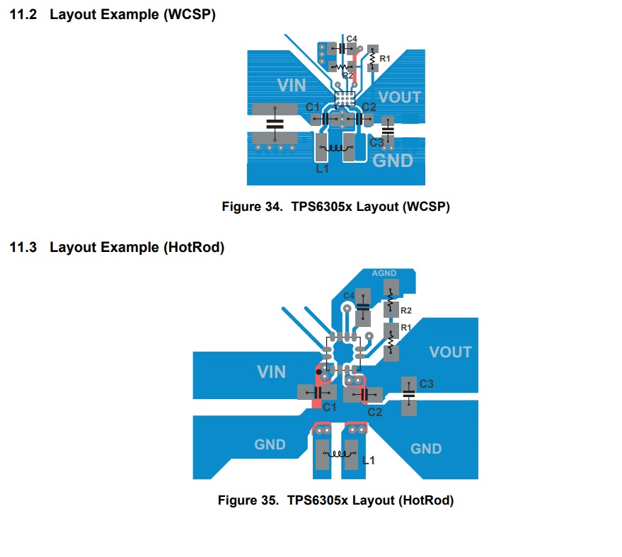
In layout example which datasheet mentioned, C1 and C2 are located between IC and L1.
If we set so, pattern between IC and L1 become little bit long. I have not seen this pattern.
Why do you set that layout? Is there specific reason?
Thanks and best regards,
Ryo Akashi
  • Hi Ryo:

    Thanks for asking.

    The layout for Cin,Cout has the 1st priority. It's very important to make the two side switch loop as short as possible.

    Besides, the package size of these two caps is very small, it won't influence the perfermance of inductance too much.

  • Hello Minqiu,

    Thank you for your reply.
    I understand Cin and Cout layout are 1st priority and the performance of inductance are not be influenced by cap because cap side is small.
    Let me ask more detail.
    TPS63030 looks similar function device.
    In this device's layout example, Cin/out loop is short. Also Inductance loop looks as short as possible.
    Is it difficult to implement similar layout for TPS63050? (Due to pin assignment, is it difficult?)
    I would appreciate you would give me comment.
    Thanks and best regards,
    Ryo Akashi 
  • Hi Ryo:

    Yes, the pin map is not same, and not easy to make all component closest to the IC.

    As far as we used, the TPS63050 with the recommend layout could work well. If you have some special requirement, please let us know and to see if it could meet or need other solution.

  • Hello Minqiu,

    Thank you very much for your reply.
    I understand recommend layout could work well so far.
    Thanks and best regards,
    Ryo Akashi