This thread has been locked.

If you have a related question, please click the "Ask a related question" button in the top right corner. The newly created question will be automatically linked to this question.

TPS51285A: TPS51285A 3.3V Output support

Part Number: TPS51285A

Dear TI Experts,

Greetings,

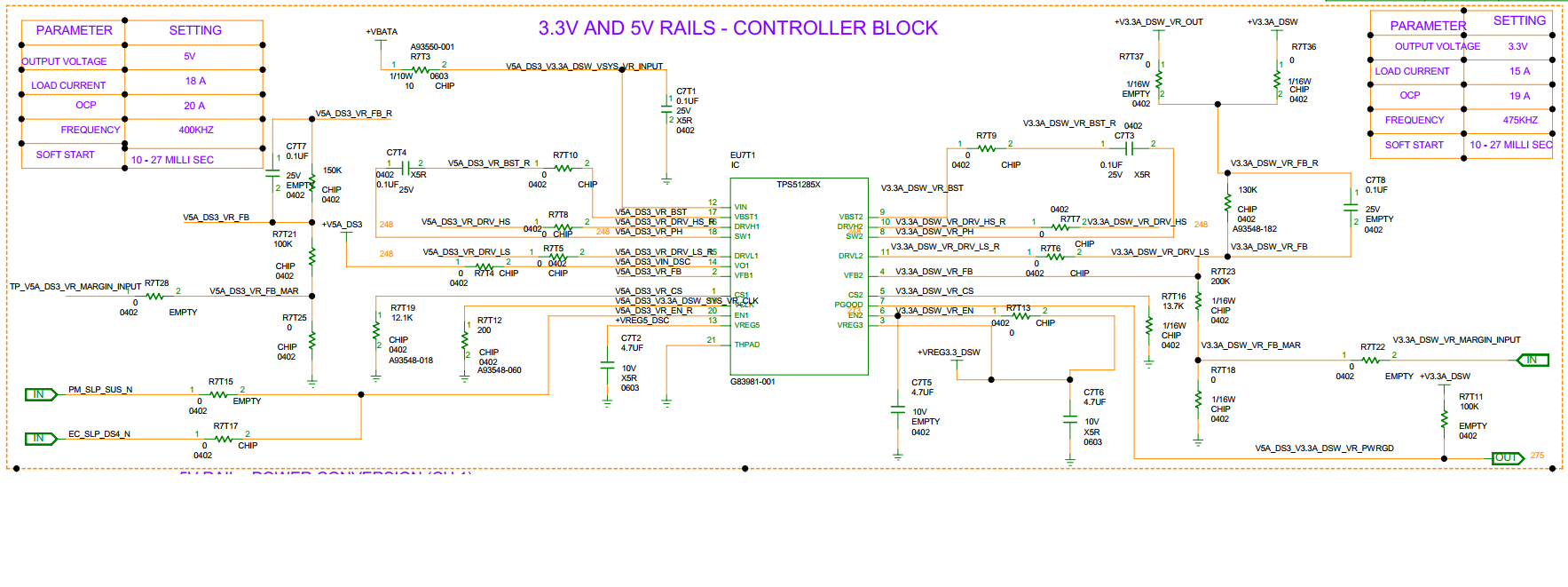
I have few questions regarding the operation of the TPS51285A. 

1. I just want only 3.3V output which is Channel 2 output so I am just giving 3.3V to EN2 pin. Will it work? Does it have any dependency on the EN1 pin or CH1 Circuitary?

2. What is function of VO1 pin of the IC?

3. Can I connect Simple RC delay to EN2 Pin which is derived from VREG3. which can give delay between VREG3 and 3.3V Out (Ch2)?

Kindly, Help in issue.

Thanks and Regards

Saunak Bhalsod

  • 1, For your first question, do you mean you only want to use channel2? If yes, suggest to do below connection.

    VBST1/DRvH1/DRVL1—open, SW1/CS1/FB1——connect to GND together with 1K resistor, EN1—connect to GND with 1K, VCLK —open, VO1—Open

    2, VO1 is used for switchover function for saving power. You can refer to page 15 for details.

    3, Yes, it is Ok

    Yuchang

  • Hi Yuchang,

    Thanks for the answer,

    However, for Point 3, when I connect RC delay of let say 10k and 4.7uF. IC is working in abnormal way and CH2 rail (3.3V) is shutting off after some time. 

    However, VREG3 is coming 3.3V.

    Please note, IC is not recovering back even I removed RC Delay Circuit and Directly Short the VREG3 to Enable pin for CH2 (EN2). 

    Can you please suggest what could be the possible reason(s) for this failure. 

    Thank you.

    Saunak

  • Hi Saunak,

    What’s the status of channel1 when this phenomenon happen? Did you tied the EN1 to GND?

    And what about the timing? Vin—>Vreg3–>En?

    Upload your schematic for review and if you have the issue waveforms (EN , Vreg3, VIn, Vout and  EN, SW, VIn, Vout), please also upload.

    Yuchang

  • Hi Yuchang,

    please see the schematic attached below,

    with current belwo design ( without delay from VREG3 to EN2) , this part works fine and impedance from EN2 pin to ground is 280K ohm. we added delay of ~80msec (R7T13-->100K & C7T5-->2.2uF) from VREG3 pin to EN2 pin, after delay controller is not working, we measued impedance from EN2 pin to ground is 300 ohm. due to this slew raise voltage on EN2 pin is there any CMOS logic internal to controller is damaging? because after delay parts are not working and even after removing delay and connect VGER3 to EN2 also parts are not recovered.

    thanks,

    Ramesh.

  • Hi Ramesh, actually I don’t think this delay can make damage happen.  

    1, Can this issue be reproduced at other borads?

    2, after the issue happen, channel1 still can work or not?

    3, need you catch waveforms as I mentioned in last message.

    Yuchang

  • Hi Yuchang,

    this issue reproduce in 3-4 boards, without delay on EN2 pin everything works fine from VR point of view, once we introduce delay from VREG3 to EN2 then parts are not booting.

    please can you share your email ID so that will start conversion over emails..

    thanks,

    Ramesh.

  • Yuchang-zhang@ti.com

  • Since we are touching by Email, this thread will be closed.