This thread has been locked.

If you have a related question, please click the "Ask a related question" button in the top right corner. The newly created question will be automatically linked to this question.

TPS7A92: Rtheta JB Question

Part Number: TPS7A92

We've noticed that the Rtheta-JB is 29.1C/W for this device TPS7A9201DSK. Comparing to the TPS7A7100RGT which has an RthetaJB of 17.2C/W

Why are the JB thermal resistances so dramatically different given the Rtheta JC specs are about the same -  is this correct?  Are there two different constructions inside? 

  • Hi Steve,

    Yes, these are very different devices and the method of connecting the thermal pad is different for the two packages. TJC is roughly the same as in both packages the amount of material to the case is roughly the same. 

    The key thermal metrics that should be used are TJA, and PsiT. TJA is used to predict the thermal rise and PsiT can be used to verify. 

    Here is an app note on how to use these: http://www.ti.com/lit/an/slua844b/slua844b.pdf?keyMatch=THERMAL%20DESIGN&tisearch=Search-EN-everything

    I hope this helps.

    Regards,

  • JCHK,

    I think the problem we are having with TPS7A9201DSKT is that the published junction to board resistance of 29.1 C/W is suspect.  If the junction to case bottom is 3.2 C/W (which seems reasonable)  we calculate the case to board resistance or about 4 C/W thru the solder joint, then we would expect the junction to case resistance to be around 7 to 8 C/W, not 29.1 C/W.

    Please advise.

  • Hi,

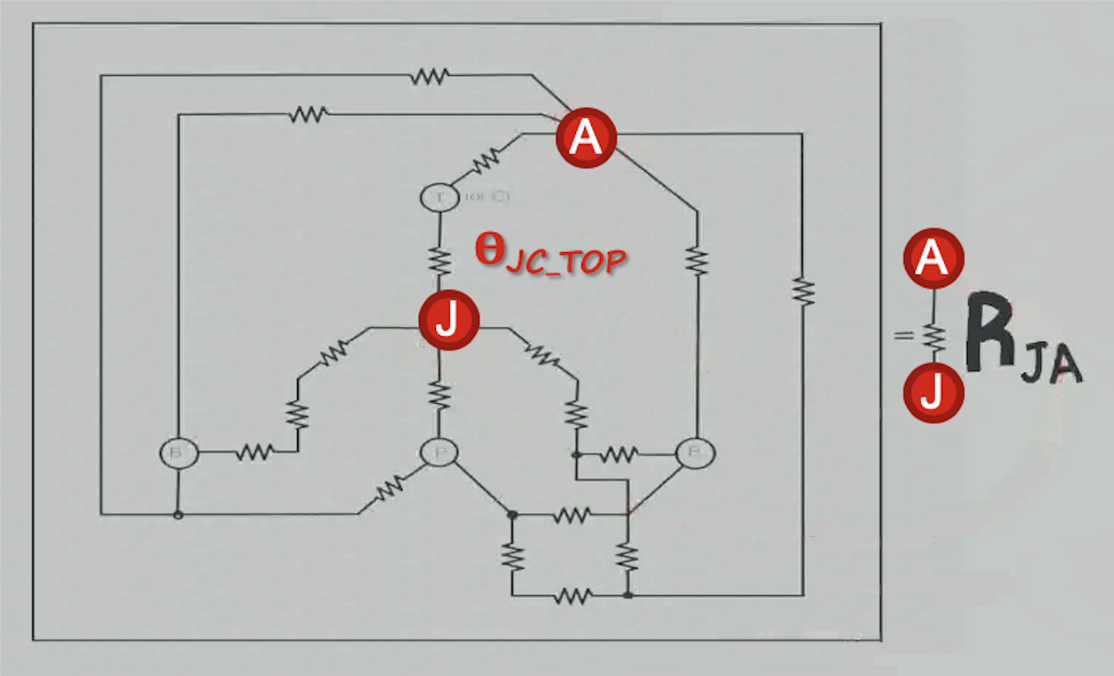
    The thermal models are based on thermal simulations using the die size, lead-frame, and package. It is actually quite difficult to measure the parameters directly as the below diagram indicates:

    This is why I like to focus on TJA and then using PsiJC to verify.

    Regards,

  • That’s all good, but it did not address my question which had to do with junction to board resistance.  Please try again.

  • Hi ,

    Unfortunately there is more that must be accounted for in the Junction to Board (Rjb) thermal metric than just the Junction to bottom of Case  (Rjc(bot) plus the thermal resistance solder. This is because Rjc(bot) is defined as the temperature of the board at the outer edge of the pin of the device. When mentally evaluating this keep in mind that what complicates the physical analysis further is that the board itself will conduct the heat provided by the LDO to other parts of the board which will results in a lower the pin temperature which mathematically results in a higher Rjc(bot).  

    Hi ,

    Regarding your question on why there is such a difference between the two devices you mentioned (TPS7A92 and TPS7A71), it is important to keep in mind the size of the devices is critically important. So while a 3x3 mm and 2.5x2.5 mm seem similar, the surface area of the TPS7A92 in the 2.5x2.5 package is ~30% smaller and while the thermal metric won't scale exactly with the surface area even just scaling the TPS7A92 Rjb by 30% gives a Rjb of 20.3C/W which is pretty close to the 17.2C/W listed in the TPS7A71 datasheet. 

    I hope that is helpful in explaining some of the intricacies of the JEDEC thermal metrics. 

    If you'd want to learn more about how JEDEC defines the various thermal models you can read our app not on it (http://www.ti.com/lit/an/spra953c/spra953c.pdf) the Rjb section starts in section 4 (on page 10)