This thread has been locked.

If you have a related question, please click the "Ask a related question" button in the top right corner. The newly created question will be automatically linked to this question.

TPS61175: Chip keeps frying

Part Number: TPS61175

Hi there,

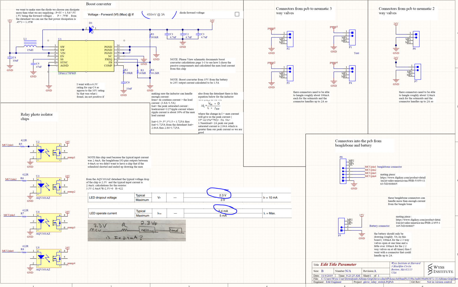
I designed a simple boost converter board with this chip. My board boosts from 15V to 24V, the 24V is then used on optocouplers which are controlled by a beagle bone's inputs to switch the solenoid valves on and off. The board had been working fine for the past couple of weeks but all of a sudden stopped working. It could be a number of variables, one being that we switched from a benchtop power supply to a battery (this one to be exact: https://www.rrc-ps.com/fileadmin/Dokumente/Data-Sheets/DS_RRC2054.pdf ) . I was hoping to get someone that is an expert on this chip to look at my schematic and PCB layout to see if there are things that might be missing that could cause harm to the chip that I didn't think about. Thank you! 


  • Hi Brittany,

    It could be helpful to provide more details about the design requirements of the boost (min max input voltages, needed output current...).

    Please provide also L1 & D1 part numbers.

    I saw in your schematic that you chose C4 rated voltage to be 6.3V which is, for sure, not sufficient to handle 15V input voltage. A 50V capacitor will be Ok. You may need also to add additional input capacitance to handle the transients of the battery.

    Regards,

    Abdu

  • Hi Abdu, thank you for your quick reply. Of course! we are using a battery which I don't actually know the min and max as the datasheet doesn't state that ( I attached the link to the battery in the previous post), My guess is it ranges from 13-17V. The needed output current of the system was about .5A and I calculated all the passive components that the chip could provide up to 1.5A output. I'm not quite sure where you saw that C4 is rated for 6.3V it is actually 25V. the L1 is MSS1038-153MLC and the diode is MBRA340T3G. I am attaching a picture of my bom as well just incase for reference. Thank you for your help! 

  • Hi Brittany,

    I'm the AE of this part.

    When the input is power supply, it is 15V right? Before you switch to the battery,  please test the battery voltage to ensure the battery voltage is not to high or low.

    One question, how did you switch the power supply and the battery? online switch or disable the TPS61175 then enable it again?

  • Hi Helen!

    I was hoping to hear from you (I didn't know how to contact you without posting on the thread).

    When you say test the voltage of the battery, do you mean to make sure it doesn't exceed the 18V input? Why would the min be a concern, since there is no way the battery would go below 2.9V.

    Also, what do you mean by how did I switch the power supply? If you are asking how did I turn the power supply on and off we just used a standard SPST switch and attached that to a dc power jack.

    Last question: do you think the fact that I didn't include any flyback diodes around my MOSFET optocouplers would have caused the chip to fry? Thank you! 

  • Dear Sir,

    Yes, you need to check the battery voltage to ensure it is not too high or too low. If the battery voltage is too low, the input current(inductor current) will be very high, if the current rating of the inductor is not enough, it may saturate.

    I need to know the sequence of how you switch the power supply to battery: turn off the power supply, then add the battery voltage through a SPST right? Did you add any inductor or capacitor after the SPST? the high voltage spike during switch the SPST may also damage the IC.   Please draw a block diagram of the power supply, the location of the SPST, battery. and the on/off sequence of the power supply, battery, SPST.

    Also I need to know  the exact moment when the IC damaged? I guess it happened just at the time when the battery voltage added.  But need you confirm.

  • By the way, could you please tell me which pin of the TPS61175  damaged? Vin pin? Enable pin or the SW pin? you can test the impedance from the pin to the GND.

  • Hi Helen, Here is a picture of how the switch and the power from the battery are attached to the circuit. I didn't add anything besides what was needed to boost the tp261175. To answer your other question. that is hard for me to answer. as I just designed the board and then was told by a peer that the board stopped working. So I do not know the exact order of operation. I was told that they were running solenoid valves from the board for several hours then turned everything off, then they turned things back on and nothing was happening. 

  • What does testing the impedance of the pin show me? What should I be expecting to see by testing the impedance of a pin?

    When I looked at the SW pin it didn't seem to be behaving as expected 

  • Dear Sir,

    Please solder the IC off the pcb , then test the impedance between SW(+) and the GND(-), also the Vin(+) and GND, EN and GND. There's an anti parallel diode from the GND to each pin, so please during the test, GND should be at - to make the test accurate.

  • Hi Helen,

    Again, what should I expect to see once I am testing the impedance? (also I am a woman, haha) 

  • Dear Lady,

    Normally, it should be high impedance, the impedance should be >10k  ohm, something like 100k ohm or even more. If you found it is <1K low impedance, then that pin is damaged.

  • Hi Helen,

    Thank you for that explanation! Is this a general rule of thumb with an IC chip in general or specific with the TPS61175 that the impedance of a pin should be high? 

  • Dear Lady,

    This is a rule of thumb. If the impedance is lower than 1k, then the pin must be damaged. Have you test the impedance yet?

  • Hi Helen,

    I just measured the pins. the impedance between SW and GND is 754ohm the impedance between Vin and GND is 1.6kohm and the impedance between EN and GND is 54ohm. would you mind looking at my schematic and layout again to see what could be causing the chip to fry? 

  • After comparing the impedance on a working chip and the damaged one it appears that the EN pin is damaged. 

  • Dear Lady,

    Thanks for the comparison.

    Yes, EN pin is damaged. But the SW to GND and the Vin to GND impedance is also low.

    I think the voltage spike(high dv/dt) during the power supply switch cause the damage. The EN pin can be damaged by a very high dv/dt.

    Add a 0.1uF ceramic as close to the EN pin as possible can help to solve the problem.  if possible, please add a 1k ohm and 0.1uF cap to the EN pin. the 1k ohm resistor also helps to reduce the dv/dt.

    Why the SW to GND impedance is so low, is this an on board test or you have removed the IC off the board? Did you test from SW to GND. (note: GND to SW can have different result)

  • Hi Helen,

    Why would I get a voltage spike if I am using a bench power supply, that doesn't make sense.

    Also, those impedance values of the SW and the VIN were the exact same on a brand new chip so that is concerning to hear that those are low (everything was tested off the board). I also don't understand how GND to SW vs SW to GND would make a difference 

  • Dear Lady,

    There's an anti-parallel diode from the GND to SW.  if test from GND to SW, then the impedance will not so high. While if test from SW to GND, it will be higher impedance.