Hi,
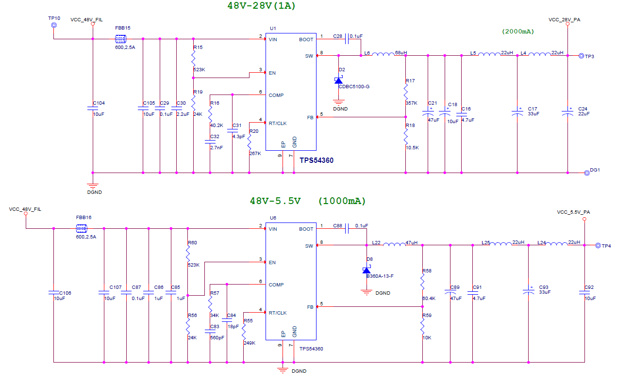
I am using 2 TPS54360 for two different voltages.
please see the below schematics for the same .
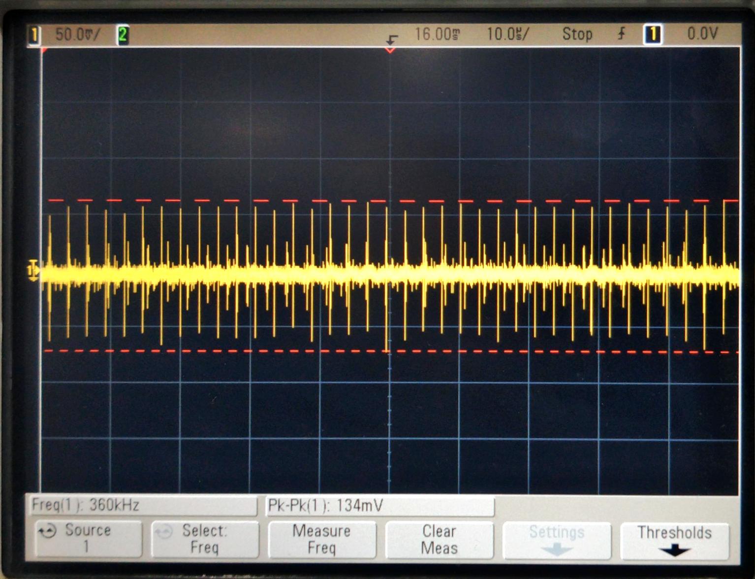
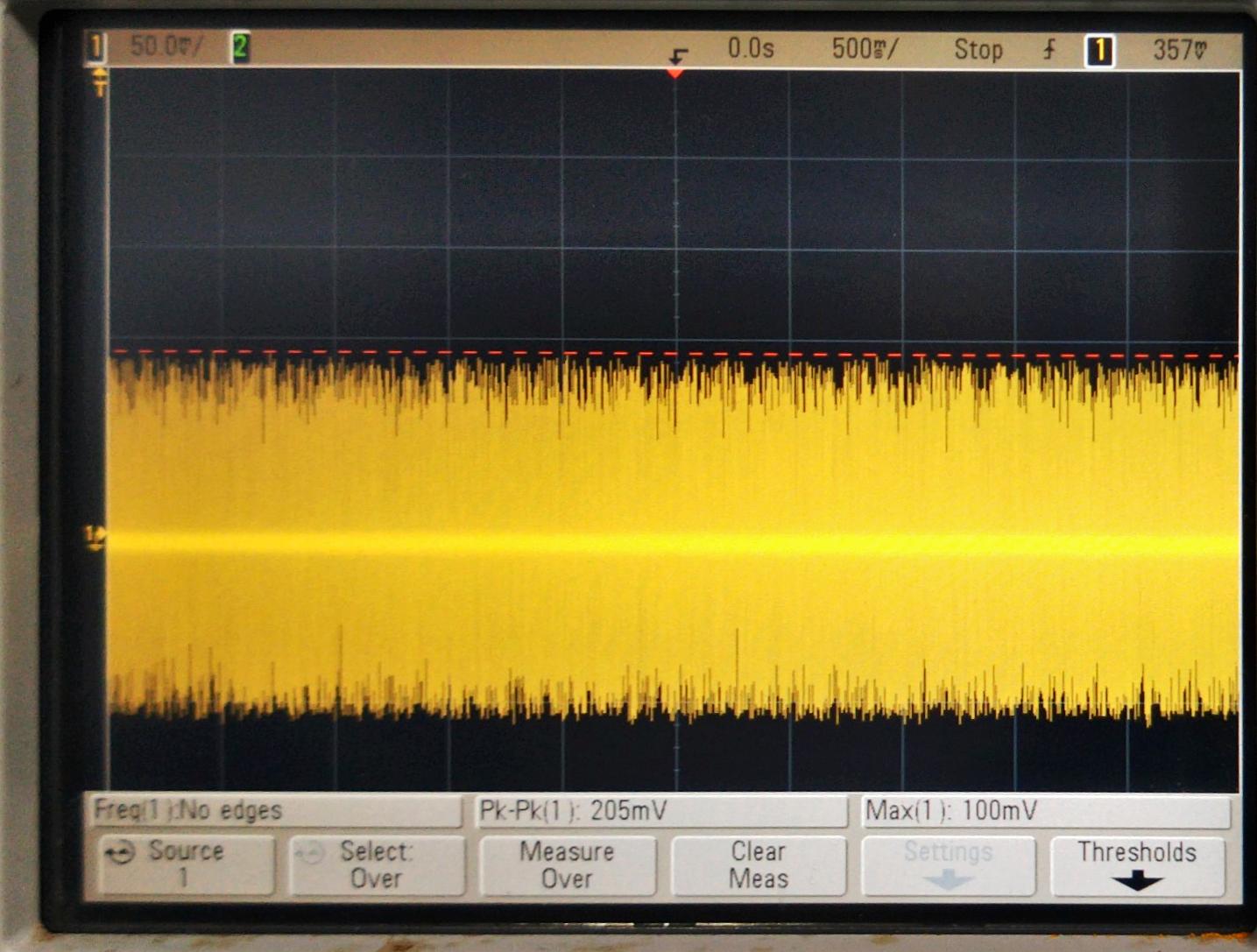
When i load the regulator U1 with 2A, I am getting noise of >200mV on the other regulator output U6.
While removing the load from U1 , The noise from U6 get disappear.
Please let me know some solutions.
Schematics ;
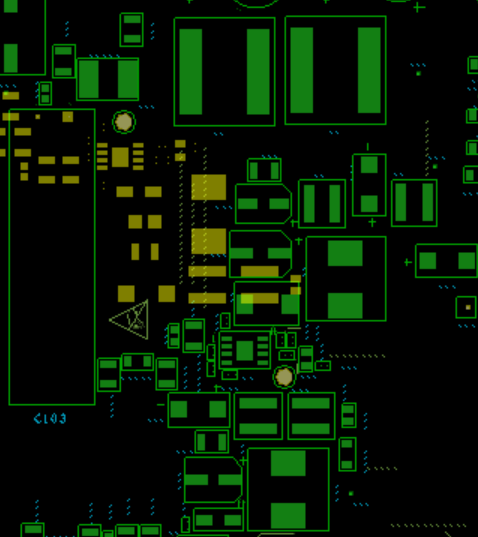
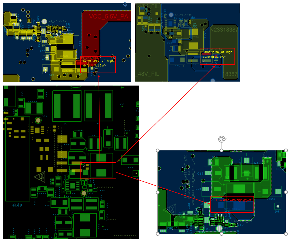
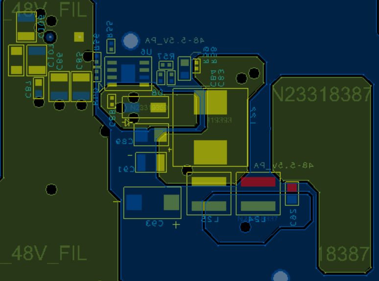
Layout ,
U1 is on top and below that we had provided full GND reference .
Screenshot for layer 1;

Bottom layer ;

Layer 3 ,power layer
Waveform for the U6 output .
Thanks,
Jaice