This thread has been locked.

If you have a related question, please click the "Ask a related question" button in the top right corner. The newly created question will be automatically linked to this question.

BQ24195: Overheating issue

Part Number: BQ24195

Hello!

We are using the BQ24195 chip within a powerbank application. 

With loads below 1.7A the chip works correctly, but if the load is higher, I meet with a voltage drop after a few minutes of work.  The temperature of the chip reaches 85 degrees.

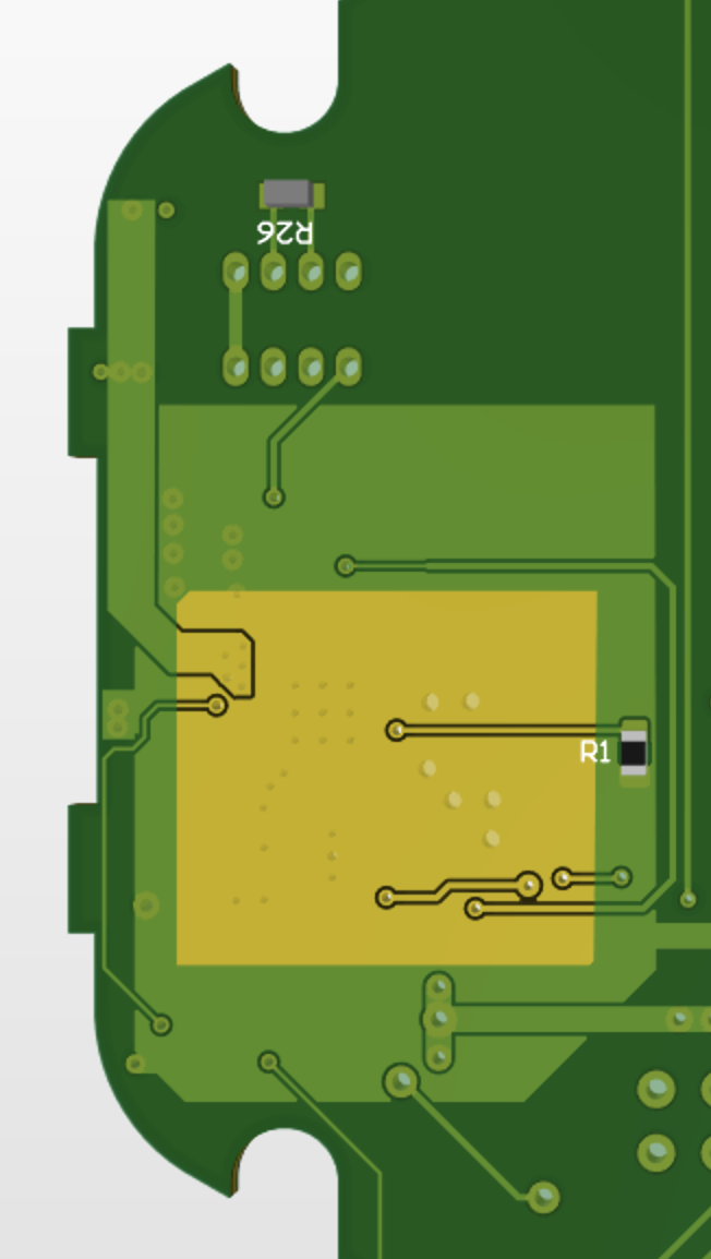
What role does the size of the PCB board play in overheating? Also, we have vias and thermal pad in our design, but we still face the problem of overheating. We've made a space with an open ground area on the top and bottom layers of the PCB to dissipate heat, which has slightly improved the situation.

I have an Evaluation Board on my hands, but I don't see this much heat under heavy loads. 

I've attached the top layer of our application, maybe you'll have some tips on how to improve the situation.

Best Regards!

  • Hi Andrei,

    How much ground copper on internal or bottom layers is connected to the thermal pad vias?  Best if you have at least 4-5 times the size of the thermal pad as a copper heat sink on the exposed bottom of the board.  

    Regards,

    Jeff

  • Hi Jeff, 

    Thanks for your reply

    Yeah, we have quite big 10X ground copper on the bottom layer, we made the square area open from the paint to increase heat dissipation. It’s problem for us to make big ground copper on the top layer, but we tried.  

    We’ve made different variations with very large ground copper on the bottom because we have space there, but it does not give the desired effect. We’ve made a 4-layer version of the board (production version is 2 layers) for the experiment, it also improved efficiency, but only by 0.2-0.3A. This and the fact that the EVM has a fairly large ground copper area on the top layer connected to the С1 С19 capacitors (only it becomes warm under load in my experiments) gives me the idea that the top layer is much more important. Am I right?

    Maybe you can recommend where to get a gerber example of design on a small PCB size that works correctly? We have a workspace about 25 square centimetres

    I'm trying to find a solution to this problem in order to discuss it with a team of engineers, as we've already done 3-4 iterations in an attempt to win 

    Thank you!

  • Hi Andrei,

    I do not have a small form factor layout to recommend.  I only have the EVM. 

    Creating a large, unbroken top layer copper plane is almost impossible.  A large bottom layer plan is highest priority, followed by internal layer.  Your plane looks a bit too small and is somewhat broken up.

    Are you using 2oz copper?

    Regards,

    Jeff

  • Hello Jeff,

    Thank you, I got your point of view on the increase of ground copper on the bottom and inner layers. We will try.

    No, I think we're using 1oz. Now it seems that using 2oz would be more reasonable.

  • Andrei,

    Yes, 2oz copper will be much better at heat sinking.

    Jeff