This thread has been locked.

If you have a related question, please click the "Ask a related question" button in the top right corner. The newly created question will be automatically linked to this question.

TPS7B67-Q1: IC failure--schematic review

Part Number: TPS7B67-Q1

Hello team,

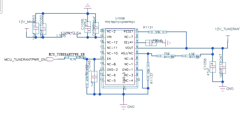
Could you help review the schematics that customer use, 12V main means the 12V bat (9v-16v typical), is there any risk?

Customer report 7pcs IC failure in 0km vehicle, FA is ongoing. 

One of my concern is the low dropout recovery issue of tps7b67, is it possible the output is higher than the input during the start up, which cause a reverse current that damage the device.

Thanks.

Dongbao

  • Hello Dongbao,

    I will respond to your question within 2 business days.

    Thanks,

    - Stephen

  • Hello Dongbao,

    Can you please provide the failure that is being seen?

    I understand that 7 IC's have failed, but how have they failed?
    What is the symptom that indicates failure? 

    I see two items of concern.
    First, the setpoint is 12V but the input voltage spans 9V-16V. 
    The linear regulator may operate a significant amount of time in dropout, where it has poor performance.

    If this is a battery on an electric vehicle, then I would be worried about electric starting or other similar requirements which drive large transients on the battery voltage.  There is no parallel diode across the linear regulator (from the output to the input), so the linear regulator could see reverse current depending on the requirements.

    Thanks,

    - Stephen

  • Hi Stephen,

    Thanks for your feedback, FA is ongoing and i haven't got the final results, the failure symptom is the output voltage is not correct ( 8V for failure IC and 12V for good IC).

    • I know the output performance under dropout mode is not good, will it cause failure? 
    • Regarding the low dropout recovery issue of tps7b67, is it possible the output is higher than the input during the start-up?

    Dongbao

  • Hi Dongbao,

    Operating a linear regulator in dropout mode is not sufficient by itself to cause damage.

    We would need oscilloscope plots of the inputs and outputs of the LDO to better assess possible root cause of failure.
    The tps7b67 datasheet lists an absolute maximum rating on the output voltage pin of 22V.
    This is 10V higher than the setpoint, so while still possible it is unlikely that exceeding this pin rating is the issue.

    Can the customer provide oscilloscope plots of the input and output of the LDO?

    Thanks,

    - Stephen

  • Hello Dongbao,

    Since it has been a week without a reply, we assume that this issue has been resolved.  If this is not the case, please feel free to reply.

    Thanks,

    - Stephen

  • Hi Stephen,

    The FA results turned to be the internal body diode damage, however, we test the Vin and vout waveform across many conditions, i don't see Vout higher than Vin. May i know:

    1. What's the acceptable reverse current? 

    2. What's the maximum Vout-Vin limitation?

    Thanks

    Dongbao

  • Hi Dongbao,

    1. Reverse Current: Our general guidance is 5-10% of the nominal current.  So 22.5mA to 45mA.

    2. I would use the absolute maximum ratings in the datasheet table, copied below.

    Thanks,

    - Stephen

  • Hi Stephen,

    Thanks for your reply.

    1. Why the reverse current is only 10% of forward current? According to my understanding, if the gate is biased on, the mosfet will conduct in either direction. Body diode conduction should not be a concern as long as the reverse current is not high enough.

    2. The absolute maximum ratings doesn't show the limitations for Vout-Vin.

    Regards,

    Dongbao

  • Hi Dongbao,

    Linear regulators are not designed to carry a lot of reverse current through the body diode of the internal MOSFET.
    Your understanding of MOSFET behavior is correct.  However, the output voltage can only go so high in a practical linear regulator.  If there is not enough headroom between Vin and Vout, or if Vout is higher than Vin, then the internal feedback loop will try to shut off the MOSFET, not keep it on.  Even if the feedback loop turns off the pass element, the parasitic body diode cannot be turned off, so current will still flow through it.

    The limitation of Vout-Vin is due to the body diode.  If you recall the IV curve of a diode, once the forward voltage has been reached, the current through the diode rises rapidly (exponentially).  The body diode will not allow a significant amount of voltage differential between Vout - Vin, at least while it is still functional.

    Thanks,

    - Stephen

  • Stephen,

    Thanks for your reply.

    Dongbao

  • No problem Dongbao.

    Let us know if you need anything else.

    Thanks,

    - Stephen