This thread has been locked.

If you have a related question, please click the "Ask a related question" button in the top right corner. The newly created question will be automatically linked to this question.

TLV755P: 3.3V SUPER CAP Backup Circuit Problem

Part Number: TLV755P
Other Parts Discussed in Thread: TLV755

Hi All,

I have a strange problem when using the TLV755P as a brownout 3.3V backup supply. Please refer to the schematic below.

The 3.3V circuit should draw about 100mA in normal operation. The backup circuit is fed from C114 a 5F super cap. To test the circuit, I have disabled the normal 3.3V primary supply. On power-up, the super cap slowly charges from a separate 5V supply to about 4.5V through a super barrier diode D22 in series with R163 a 20R resistor.

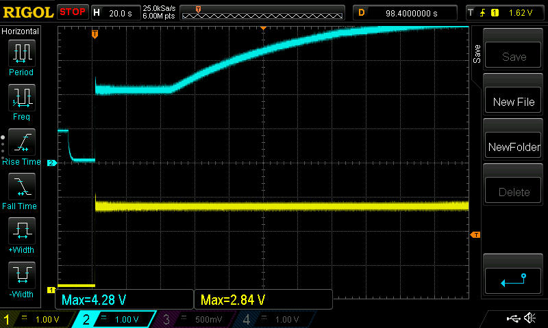
To prevent back feed from the normal 3.35V supply the TLV755P is fed with a second super barrier diode D23 such that Vin is about 4.4V. I have a 10UFD bypass on Vin and 1UFD on Vout right at the chip. When I power up, the output voltage rises to only 2.6V, not 3.3V as it should. At this point, Vin is 4.4V and drawing only a few mA. The device remains cool. If I jumper from 5V directly to Vin the output does go to 3.3V. If I then remove the jumper it immediately drops back to 2.5V again. So, it is not a start-up problem. It does not work if there is even one super barrier diode in the circuit i.e. jumpering D22 or D23 does nothing. I have tried different bypass values and different TLV chips with no effect.

I realize that under full load the 20-ohm resistor would be a problem, dropping 2 volts at 100mA. But remember the super cap will charge all the way to 5V with no backup supply load in normal operation.

Thanks in advance fo any ideas to solve this. 


  • Hi Dan,

    I will be reviewing your circuit and question, and I will have at least my first response within 2 business days.

    Thanks,

    - Stephen

  • Hi Dan,

    Can you provide oscilloscope plots of the Vin signal and the Vout signal during turn on?
    Another oscilloscope shot of these signals during steady state just to rule out any abnormal behavior would be helpful.

    Can you confirm the voltage rating of the output capacitor?

    Thanks,

    - Stephen

  • Hi Stephen, The output cap is a 50V ceramic. See enclosed scope power up view.  The super cap charges (takes several minutes),Vin rises quicky to 2.6V, Vout approx. equals it.

    Then Vout kinda limits at ~2.8V. Blue trace is Vin, Yellow trace is Vout. Hope this helps. Regards Dan

     .

  • Hi Dan,

    Can we get 3 additional oscilloscope plots?

    1. A zoomed in version of the spike, seen above, around 20s into the first plot.

    2. An oscilloscope shot showing the shutdown waveforms seen at the very left of this scope shot.

    3. A steady state scope shot of the Vin and Vout, with the intent on showing any ripple that may be present (if any).

    Thanks,

    - Stephen

  • Hi Stephen, The bottom line is that the reg does not work when fed through a diode.

    As you probably realize the spike at first powerup is feedback into the "dead" 3V supply due to the fact that the 5V supply comes up feeding back into the 3V via chips on the PCB. This is NOT a normal condition. In the working circuit, the 3V supply comes up first. So the spike you want to see in detail (plot 1) does not occur in the working circuit.

    On the very left, (your plot 2 request) the pre-trigger, is me manually bleeding off the super cap before powering on. This does not happen in the real circuit. It should be fine to have some charge on the super cap at power on. I just bleed it down for a proper initial state.

    In the original plot I sent, once the super cap charges above the 5V feedback voltage, Vin becomes the current source for the 3V backup supply. But still, the reg. does not seem to turn on correctly. The plot below shows the same powerup sequence with additional jumpering 5V directly into Vin (two times in the plot). Notice the regulator functions correctly until the 5V is removed. This seems to indicate the regulator has NOT been glitched.

    In the following plots, BLUE is Vin, YELLOW is Vout.

    The next plot shows a power failure with 3.3V primary enabled. As you can see,  as expected Vin has stabilized at full 5V under no load. Notice the 3V supply immediately drops off to 2.8V while Vin is drops very little. However, a telltale sign is an oscillation seen on Vin indicating the reg is unstable for some reason (I think this would be indicative of your plot three request?) BTW in this plot,Vin is bypassed with a 10mfd and 1mfd ceramics within 1/4 inch distance from the chip. Vout is bypassed by 10mfd within 1/4 inch of the chip and a lot more bypass on the PCB.

    The next plot is Vin 11Khz ripple zoomed.

    Thinking it could be some strange interaction with the super barrier diode I substituted D23 with an ordinary 1N914 and other that a higher drop and deeper oscillation (seen above), it does exactly the same thing. Even adding 100mfd radial electrolytic in addition to the ceramics on Vin fails all be it with lower ripple.

    I don't know how to bypass the reg. so that it will work with a series diode in the circuit.

    Regards, Dan

  • Hi Dan,

    I am reading through your posts.
    You have provided a lot of quality data and I need to absorb it.
    On first glance there does not appear to be anything wrong with the design, and that the LDO output should regulate.
    I have some ideas on what might be happening but I wanted to understand all of the oscilloscope waveform 'bumps' before looking at some things on my end.

    I will reply back soon with additional feedback.

    Thank you for your patience.

    Thanks,

    - Stephen

  • Hi Dan,

    Can you please short out the diode D23 and confirm that the issue is still present?
    An oscilloscope plot would be helpful.

    In the meantime we are sending this to one of our designers for review.
    Please give us a few days to look into this further.

    Thanks,

    - Stephen

  • Hi Dan,

    Can you confirm that the 11kHz oscillation goes away when the 5V is directly applied to the LDO input?

    If the oscillation is still present with 5V directly applied, can you confirm your load capacitance?
    Manufacturing part numbers are helpful, so I can build an equivalent model of the load impedance for our analysis.

    Thanks,

    - Stephen

  • Hi Stephen, First let me say I really appreciate the time you are taking to help me out with this problem. Yes, the Vin oscillation goes away if I short 5V to Vin. However, in a real power fail i.e. there is no 5V supply, just a charged super cap, if I short D23 to the charged super cap, the oscillation goes away BUT the regulator still does not go into regulation. So, my previous assertion the reg does not like diodes in series with Vin is wrong. It seems the super cap itself is at least part of the problem. AVX PN SCMT22C505MRBA0. Its ESR is just 150mOhms and a peak current of 7Amps.

     http://datasheets.avx.com/AVX-SCM.pdf

    I was also wrong in my assertion that the feedback voltage is not relevant in "normal operation" power-up. In that case, the primary 3V supply will feedback into Vin before the super cap charges. So I am providing that power-up plot below.

    Again, Blue is Vin, Yellow is Vout. The beginning transients causing a trigger is the mechanical switch closure, followed by the SMP soft start, nothing seems unusual. There is also some HF noise from the switcher which is almost all common mode (100mV) due to convenient probe ground position.

    The actual Vout cct capacitance is complex, 2 x 22MFD low ESR caps on the switcher output plus about 50 x 100N caps distributed over the PCB. The 3.3V also creates 3.3Va through a ferrite bead and a 100UMFD tantalum cap. (C157) (now 10MFD)

    When Power is off, the primary 3V SMP Vin side also becomes part of the load so there is one more 22MFD cap on it (C108). SMP Vin is blocked from the 24VDC supply by an FM4934 (D45) diode. Here is pretty much the full schematic of the relevant power supplies. Unfortunately, it would be very difficult to isolate the downstream parts of the 3V supply for analysis. 3.3V is an inner PCB layer plane.

  • Thanks Dan.

    This is extremely helpful in understanding what might be happening.
    We are also wondering if the large input capacitance is making an impact, but it will take some further work on our end to know for certain.

    I reviewed the super cap earlier today and noticed the ESR.
    It's similar to a dry tantalum or that sort of capacitor.  Nothing unusual for what we would expect to see.

    I have 10 pieces of the TLV755P on order that you are using, and we have plenty of boards to install them on, should we need to do any bench testing.
    The samples should be here in a week.

    For now, we will need a bit of time to complete some work on our end.
    I'll reply back in a handful of days on progress, so you know we are still reviewing the issue.
    If we have a result before then we will reply as soon as we have that.

    Thanks for your patience.

    Thanks,

    - Stephen

  • Thanks Steven, There is no rush on this issue. Take your time. It will be interesting to see what you can find. Just for fun, I substituted the 5F cap with a 1000MFD. It can't hold the supply long, but it clearly does exactly the same thing. Strange. Blue is Vin, Yellow is Vout.

     does 

    Regards,

    Dan

  • Hi Steven, Oops, I would like to apologize for wasting your time. My "investigation" was futile. It turns out the ground pin on the TLV755 chip was never connected. There was a hairline crack in the PCB trace right at the chip ground pin. I only found it when I finally decided to probe the ground directly at the IC pin instead of at a nearby via. With that problem fixed, the circuit works beautifully.

  • Hi Dan,

    I'm glad we were able to resolve the issue.
    Should you need any further assistance on any of our TI components, please do not hesitate to send us a question on E2E.

    Thanks,

    - Stephen