This thread has been locked.

If you have a related question, please click the "Ask a related question" button in the top right corner. The newly created question will be automatically linked to this question.

TPS560430: The devices does not start by some of the board assy

Part Number: TPS560430

i have 20 board made which are powered by TPS560430 chip, 2.1MHz PFM version.

 13 of them are working and 7 of them are not.

  All 20 boards (PCB and Assy) are finished at same time.

The details of what have been tried as the file below.

   Seems the non-working chip has a shoot through the high and low side mosfet.

Why we have this issue and how could we fix it?

TPS560430问题描述.docx 

  • Hi guys

    here is the updated attachment, with updated details and translated into english.

    Thank you.TPS560430问题描述EN.docx

  • Hi Bing,

    1. For the abnormal board, Vin is ring. I agree to remove R51, it has too large voltage drop. You can solder a 470uF/50V parallel with C42, to make Vin stable.

    2. What is the saturation current of L6? the SW waveform is the same with output waveform, is the SW waveform measured correctly? You can alsoremove C41 to have a try.


  • Hi Neal,

    Thank you for your reply.

    I did try to remove C41 and all of the load, which does not change anything.

    The saturation current of L6 is 3A, Bourns SRN6045-100M.

    Compare the working Assy and non-working Assy, Physically i do not see any different, all PCB , Components , and STM assemably are same batch.

      i had cleared up one of the non-working Assy and eye checked on PCB board, i do not see any different.

    the normal load of the 5V is less than 100mA, or for a 24V input, 10Ohms resistor should not be a issue for the input side. 

      and compare to the working version, i do not see the ripple current are exist on R51.

    So i kind of strange where is the current went to in the non-working Assy,

      Since the 5V load are verified with a standard alone power supply, 

    i am question, is that current went thruogh the mosfet from Vin to GND inside of the TPS560430 chip.

    i will try to move the 470uF cap from output side to input side for another try, but i don't think that's the reason, since i have 100% good board for 1st batch Assy, and 13/20 good board for the 2nd batch Assy.

    i had worried about the stack of the PCB, since we had the chip working well at different load with a 2 Layers PCB, the stack or GND plane should not be a issue.

  • Hi Bing,

    Well, I do think it is the outside configuration problem. From your waveform, we can see that Vin is ring. So I do recommend you to consider my suggestion and hope it helps to solve the problem.

    remove R51. solder a 470uF/50V parallel with C42, to make Vin stable.

  • Hi Neal,

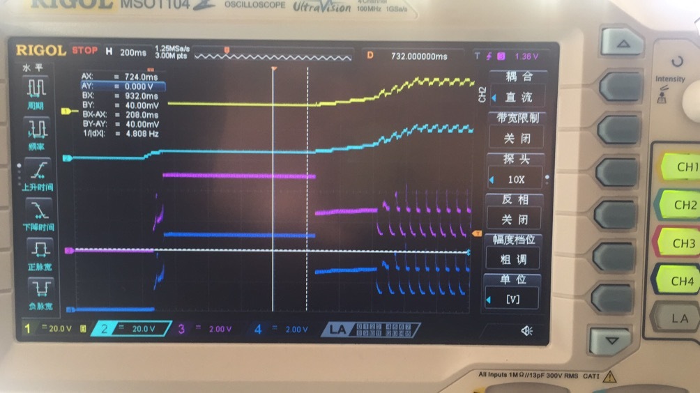
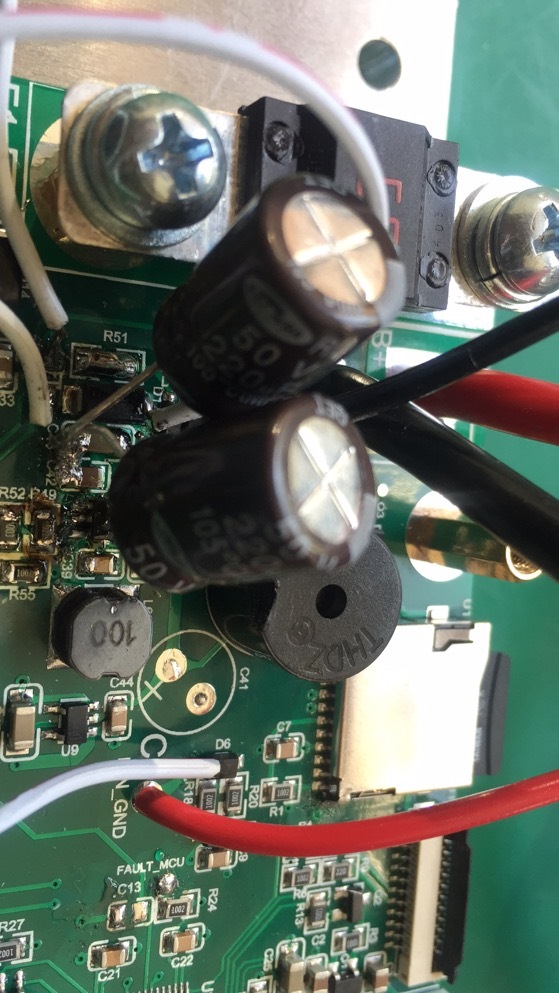
      Having 2 of 220uF cap in parallel with C42 , short the EN pin to Vin, remove the 470uF from output side, we have the o'scope result as below.

        Where, 

     Yellow: Vin

    Blue : EN

    Pink: SW

    Dark Blue:Vout

    The power supply been set as 24V output with 500mA current limit.

    Still , i don't think there are something wrong in theory, but some little details where we are missing.

    Anything else can we go for check or do you have any suggestion?

  • Hi,

    Yes it is quite strange.

    1. Vo has already rise to 5V and then Vin keeps 5V for 1 second.  Is there any other load connected to power supply other than TPS560430?

    2. After 1s, Vo suddenly decrease. Do you have any idea what will operate after 1s? Does something connected to Vo and operate 1s after Vo rise to 5V?

    3. Clearly the SW waveform is wrong. It is the same with Vo. I think you didn't measure correctly. SW is pin 6 of IC, or you can stick probe to the sw node of C39 or L6.

  • Hi Neal,

    Sorry for the late of reply.

    i have looked back to the orginal document I  asked (Link:http://e2e.ti.com/cfs-file/__key/communityserver-discussions-components-files/196/TPS560430_EE959898CF63F08F_EN.docx)

    If we look at the C-1 pictures, compare the same batch working Assy and non-working Assy, I would believe the design of the schematic and/or layout should be right, otherwise all those Assy should have issues instaed of 7/20 have issues.

    If we review the C-1 pictues, if we use the R51 as a current sensor, we will see that for the non-working assy, the Vin voltage could drop down to like 15~19V level(which the point of turn off order for EN control), which means at that time, it's could be (24-19)V to (24-15)V / 10 Ohms current goes through the R51 which is about 0.5~0.9A.

    and let look at the C-3 picture 2, the EN has been pull up, the Vin drops to about 5V which means 24-5=19V at the R51, which means about 1.9A went through the R51.

    If the internal Mosfet of TPS chip have a short through, there will be a 0.45+0.24Ohms in between Vin and GND (at 12V 25C), consider the temperature of TPS should went high and the Vin has only about 5V , the short through resistor could went higher , for example like 1Ohm, which means if there are 1.9A current went through the Vin and GND via those two mosfets, there should be about 2V in between Vin and GND.

    Is there a possible the mosfets inside the TPS chip are not working in the saturation area causing this issue?

    At which condition, the short through could happen by some outside signal effect? 1.9A is a huge current ,but not reach the Isat of the inductor yet.

    BTW: the load side had been powered by a AC/DC power supply for testing, which is working well at 5V around 0.1A DC.

  • Hi Bing,

    Your analysis is correct on condition that, the 24Vin keeps constanct. However, I believe it's not. See C4.2. 

    the IC should not have problem, and I think we should first figure out why input power supply is ring. 

    In my last response I suggest you to use big cap to stable Vin, but problem still happens. So I asked you 3 questions.

    Please send an email to me: neal-zhang@ti.com for further discussion.