This thread has been locked.

If you have a related question, please click the "Ask a related question" button in the top right corner. The newly created question will be automatically linked to this question.

UCC27517A: Mosfet Source to IC Ground connection when there is Current Sense resistor between MOSFET source and Battery Ground (BMS)

Part Number: UCC27517A

Hi,

Using UCC27517A   to drive Low side Mosfet in our  BMS system.  

Have a Current Sense Resistor between Mosfet Source  to  battery ground. Battery ground  is  all digital logic ground.

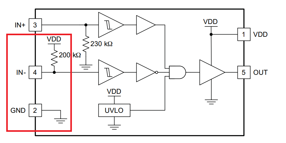
For UCC27517A, as per my understanding,  I should connect pin2 (GND ) to power supply ground  which is battery negative and pin5 (OUT) to  Mosfet Gate,  pin 4 (IN-) to  Mosfet Source. .

Current sense resistor is connected between  mosfet source and battery negative.

Are pin 2 and pin 4 shorted inside IC ? 

Is it OK to connect both pin2 and  pin4 to Battery  negative ? ( with sense resistor between battery negative and mosfet source.)

Already designed a board with pin2 and pin4 to mosfet source with  all other power section to battery ground.  It is working functionally. Seeing micro controller failure during field trial on a few boards. 

Thanks & regards,

Anil

  • Hello Anil, 

    Thanks for your interest in our driver. 

    Please refer to our block diagram below showing the internal connections of pins 2 and 4 of the IC. 

    As for your application, If not NDA restricted, please share schematic or at block diagram for my clear understanding of the driver's use or share schematic via private friend request email.

    As for the 2 and 4, they may connected to sense resistor as shown below keeping in mind that IN- (pin 4) cannot handle transients beyond -6V as it will likely damage the device. If you expect negative voltage from the battery negative terminal, parasitic current could flow through pin 2 and 4 and couple back to the controller ground referenced output to possible damage the controller as well. 

    I suggest you review your power ground to determine what voltage you would expect during normal operation.

    Regards,

    -Mamadou

  • Thanks Mamadou for the details.

    Please find attached here my schematic  section related to mosfet driver.

    My concern is related to  pin2 and pin4 connection of IC2.  Could you please review this and  suggest whether  this is OK or what change has to be done.

    Max continuous  current through shunt resistor is 40 A and peak current  will be 250A. Voltage at shunt at peak current will be  250 mV (Rs = 1 mohm ).

    Thanks in advance for the help.

    Regards,

    Anil

  • Hello Anil,

    Please add a second decoupling capacitor >=1uF in parallel to C45 and C54 for adequate noise filtering on the supply.

    You could've simply referenced IC2 to GND as well similar to IC3 rather than FGND given that it is not continuous switching application. Otherwise from the gate driver standpoint, I do not see any specific concerns with pin 2 and 4 connections.

    Regards,

    -Mamadou

  • Hi Mamadou,

    Will add capacitors.

    Are you suggesting to connect both pin2 and 4 to gnd for IC2 or

    Pin2 to gnd and pin4 to fgnd ?

    Thanks,

    Anil

  • Anil,

    Connect both pin2 and pin 4 to the same GND connection. 

    Regards,

    -Mamadou

  • Thanks a lot Mamadou for the details.

    Tested in this configuration and it is working fine.

    Regards,

    Anil