This thread has been locked.

If you have a related question, please click the "Ask a related question" button in the top right corner. The newly created question will be automatically linked to this question.

BQ77915: BQ77915 Cell balancing

Part Number: BQ77915

Hi there,

I'm asking about your device BQ77915 and its balancing algorithm.

I'm not expert and probably is my fault; but in my opinion the DS is a bit poor regarding this feature; it's a bit short and seems that some data is missing.

Attach you can see a picture with two page from the BQ77915's DS.

I assume that to trigger the internal FET balancing is required (besides no alerts and charging mode):

1) Some CV greather 3,8V.

2) Some CV greather that VCBTH.

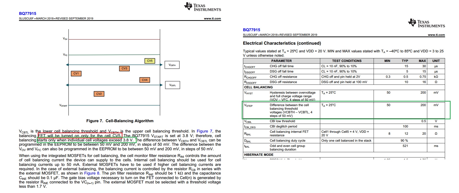
But the 2) implies by itselt the 1), it isn't? Or maybe not; because the DS show the DIFERENTIAL VALUE, I mean (VCBTH-VCBTL) but doesn't speak about the ABSOLUTE values of this limits.

So the difference (VCBTH-VCBTL) can be programmed via EEPROM, 50mV,100mV,150mV and 200mV. OK, but:

- WHERE THE ABSOLUTE VALUE  OF THEM, ARE EXPLAINED?

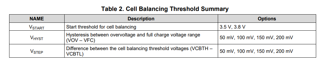
- Regarding the picture,  I assume that, if the CV5 is reduce to a value between VCBTH and VCBTL the cell balance continues. If continues reducing below VCBTL, then stop the cell balancing. I'm right?

- The VCBTH-VCBTL seems to be programmed into the buit-in EEPROM. Can I access to the EEPROM? I think not because there is not a I2C channel. Then I have to access to my Local representative to order a device with my desired VCBTH-VCBTL step? The  "Device Comparison Table" (page 3) show 4 variants BQ7791500..04, but what happen if I need other values?


thanks a lot

  • Hi Albert, 

    The cell balancing algorithm of the device is quite complex, here is a video we made that should help clear things up:

    https://training.ti.com/how-cell-balancing-feature-works-bq77915

    The cell voltage at which the cells begin to balance is configurable by the TI factory. It can be either 3.5V or 3.8V. Check the device configuration table for each device's configuration.

    Once that requirement has been met, the device will evaluate the cell voltage values and balance accordingly. This behavior is described in the video, but let me know if anything is still unclear. 

    These values are all determined by the EEPROM which is configured by the TI factory. There is no way for the user to access these values. We cannot configure these values to be something other than what is described in Table 2 of the datasheet.

    Please let me know if you have any additional questions!

  • Ok understood.

    According to Table 2, seems that there are a lot devices available.

    But according to Device Comparison Table, regarding the VStart, Vhyst and Vsetp, only two options available: BQ7791500,01,02 (3.8V 100mV 100mV)      or     BQ7791504 (3.5V 50mV 50mV)

    I'm right?

  • Hi Albert,

    We only create new configurations of the device when there is a specific request and a business need. Table 2 shows the capabilities of a new device. The BQ77915 is our most recent battery protector, so we are still building our portfolio. Continue to check the device comparison table to see the newest releases. 

  • Ok understood. And my end question, it's a bit more general. I would like to know your impression.

    My pack is a  4S3P with its own BQ77915. I need this BQ77915 overall for the balance and protections features.

    But my application will use up to 10packs in series!!!! That's means 10 BQ77915. One BQ77915 for each 4S3P.

    I'm worried about the balance features. Of course inside each pack the balance will run; but probably between packs the balance could be different. I mean that, the cells inside the same pack will be balanced properly; BUT between packs could be difference.

    In order to avoid this, here my idea:

    - Use the BQ77915 with an external mosfet and get a big discharge current on the balance circuit.

    - My idea is force the balance circuit to work in the first step, or several steps but reduce them to the first step along the charge and discharge cycles.

    Or course this is not really efficient, but this won't be a problem.

    What do you think? It's a reasonable plan or maybe not?

    Thanks a lot for your time

  • Hi Albert,

    Typically, when we have more than one BQ77915 in a system, we will "stack" the devices. See section 9.3.13 of the datasheet for more details. This involves connecting several of the device's pins together to coordinate the system. One of those pins is the CBO pin. The CBO pin will be 0V if the device is currently not balancing, and 1V if the device is balancing. This output is connecting to the CBI pin of another device. This way, you can coordinate the balancing in your pack.

  • Hi Shawn,

    Seems that link the CBO to CBI along the stack is just to inform to all BQ devices, if there are some fault.

    Seems that this link is a safety feature, it isn't?

    Nevertheless, I would like to ask if this link improve the balancing cell beetwen BQ devices. What do you think? I think no.

    Inside the same BQ the cells will be balance at the same target voltage. But what happen between two (or more ) BQ device?

    In stack topology, will be balancing all the cells at the same voltage target? What do you think?

    thanks

  • Hi Albert,

    I understand your concern. The CBO and CBI pins make sure that the devices in the stack balance at the same time. The CTRC and CTRD pins inform the lower devices of a fault in the upper device. 

    However, I suppose it is possible that one device could have cells that are more out of balance than the rest. To prevent that from occurring, my best solution is using a high balancing current. Our device supports cell balancing currents up to 50mA, and for greater than 50mA we recommend using external cell balancing FETs. This configuration is shown in figure 8 of the datasheet.