This thread has been locked.

If you have a related question, please click the "Ask a related question" button in the top right corner. The newly created question will be automatically linked to this question.

BQ24104: BQ24104 overheating problem

Part Number: BQ24104

Hello experts.

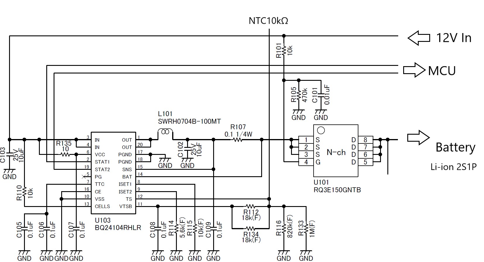
Our battery-pack products have BQ24104  battery charger IC .
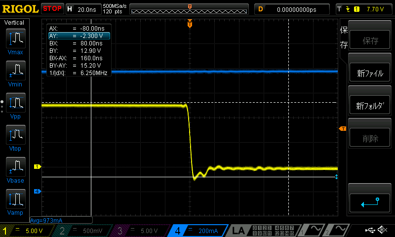
Now there is an overheating problem with BQ24104.
The package surface temperature is more than 90℃ and STAT pins output error.

Not all products have problem, most of them are normal(package temp is around 50℃), but a few products have this problem.
We want to know the cause and countermeasure.

In our circuit, Vin=12V and charge current is about 1A. battery is 2Cell(8.4V) Li-ion.

Our circuit is designed with reference to specsheet Fig16, but there are some differences:

  • N-MOS FET between RSNS and BatteryPack+. Gate and Vin, Drain and BatteryPack+, Source and Rsns are connected. FET turns on when 12V input.
  • D1 is not mounted
  • 10Ω resistor between IN and VCC
  • RISET1=10k、RISET2=5.6k
  • STAT1/2 are connected to MCU with external PU resistor.
  • PG is open
  • Hi Ramu,

    For the hot devices, are they still operating correctly, providing at least some current to the battery? Can you send a scope shot of the OUT, IN and BAT pins of a good and bad IC?  If you replace the IC on the bad boards, does it function normally?   The device is heat sinked through its powerpad.  Is the powerpad soldered down well to the PCB?

    Regards,

    Jeff

  • Hi Jeff

    Attached image file is scope shots of OUT, IN, BAT pins of good and bad IC.
    Switching waveform of Vout of bad pcb seems to be good, but current is too large.

    I exchanged good and bad ICs. The result is as follows:
    Good PCB + Bad IC -> Overheating
    Bad PCB + Good IC -> Normal

    I think PowerPad is well soldered to the PCB because the board on the back side of the IC is also hot.
    I also attached PCB layout. Is there anything to be improved?

  • Hi Ramu,

    I assume the bottom layer is a large ground plane?

    From your scope shots, it appears that the power FET from OUT to GND is shorted. With no power at IN or BAT, what is the resistance per ohmeter from OUT to GND on a good and bad IC?

    Regarding your PCB, can you send the schematic?  I don't understand the R and C components from IN to OUT. Also, the capacitor from IN to GND should have a very low resistance connection from IN pin to GND pin.   

    Regards,
    Jeff

  • I measured resistances of IN-GND, OUT-GND and IN-OUT by using multimeter

    IN-OUT resistance on bad pcb is smaller than that of good pcb.

    Probe + Probe - Good PCB Bad PCB
    OUT GND 1.9M 1.9M
    GND OUT 380K 360K
    IN GND 270K 280K
    GND IN 260K 270K
    IN OUT 970K 500K
    OUT IN 2.0M 2.0M

    > I assume the bottom layer is a large ground plane?

    Yes,the bottom layer is a large GND plane.

    Below image is the schematic.

  • Ramu,

    Your layout shows C100 and R100 from IN to OUT but I don't see those on the schematic.  Are they installed?  I don't understand their purpose.

    If not installed, the only other issue I see with the layout is the long ground return path for C103.  Can you take a scope shot of OUT, IN, either IN or charger current, zoomed in to see 1-2 pulses at OUT?  Please turn off BW limit on the OUT probe channel.  I am looking for ringing on either the rising or falling edge of the OUT pulse.

    Regards,

    Jeff

  • Hi, Jeff

    Sorry, I uploaded older layout data. Actually there are not C100 and R100.

    I took scope shot of OUT, IN and IN current. there is no significant difference between good and bad PCB except DC level of IN current.

    Good PCB  (Yellow : Vin, Cyan : Vout, Blue : Iin)

    Bad PCB

  • Hi Ramu,

    To confirm, the charge current is still accurate at 1A but the input current is higher, resulting in bad efficiency and IC heating?    If so, based on your experiments, the IC appears to be damaged. 

    The undershoot in the scope shots appear to be significant (3V?).  Very bad layout can cause that but your layout is not that bad, in my opinion.  The IN capacitor needs to have a shorter connection to IN and GND pins.  If you want to continue experimenting, you can add a Schottky diode as close to IC OUT and GND pins as possible to clamp the undershoot and see if more units are damaged.

    Regards,

    Jeff


  • Hi, Jeff.

    > To confirm, the charge current is still accurate at 1A but the input current is higher, resulting in bad efficiency and IC heating?
    Yes. Charge current is 1A but input current of bad IC is too high. efficiency of bad ic is low.

    The undershoot of OUT pin in the scopeshot seemed to be larger than it really was, due to bad measuring method.
    I improved measuring method and the undershoot became smaller as shown below. However it was -2.3V, exceeding absolute maximum rating : -0.3V~20V.

    After adding schottly diode on OUT pin, undershoot became -1.7V, but It's not enough.Do you think improving location of IN capacitor reduce undershoot and risk of overheating?


    * ch4 is not measured

  • Ramu,

    I apologize for the delay due to the holidays.  Any progress on debugging?  The new scope shots are not bad, as you noticed. 

    Regards,

    Jeff

  • Hi Ramu,

    Any update on this?

    Regards,

    Jeff

  • Hi Jeff,

    Sorry for delay.
    We think we need to make new board and test.
    We are planning to make prototype board incorporating the following improvements:

    • Add a schotkey diode between OUT and PGND.
    • Improve ground return path for C103.

    If you have any other ideas for improvement, please let me know.

  • HI Ramu,

    Those changes should reasonable.  Keep me posted on the results.

    Regards,

    Jeff