This thread has been locked.

If you have a related question, please click the "Ask a related question" button in the top right corner. The newly created question will be automatically linked to this question.

UCC25600: waveform, dead-time,

Part Number: UCC25600

Hello.

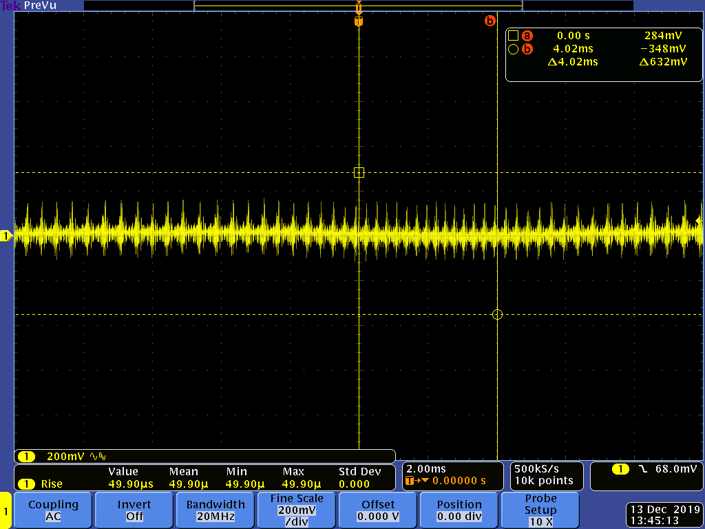
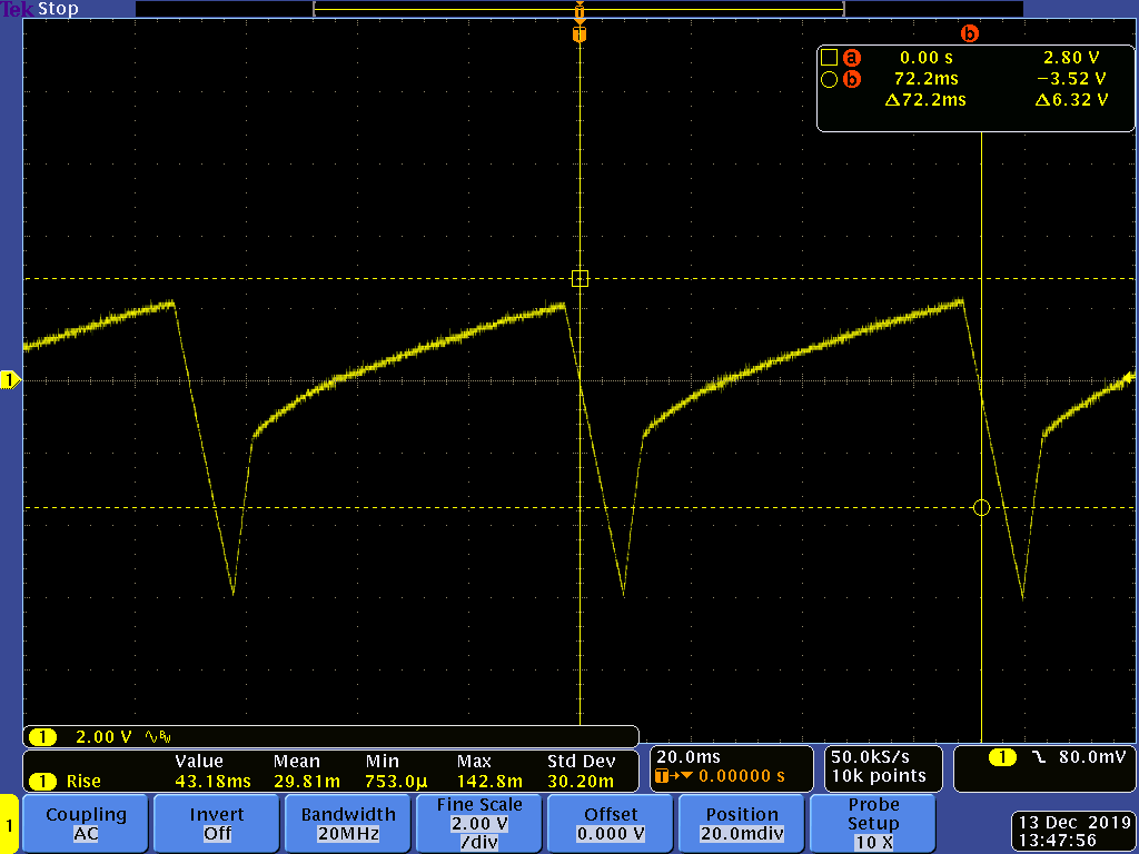
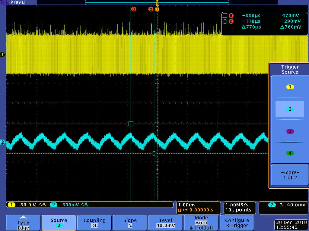
I am testing a 2kW LLC converter using UCC25600. The following waveforms appear during the test with a variable output voltage in the range of 43V to 56V.

In 54V operation, it is designed to enter burst mode at about 1A.

The following waveform is generated near 43V / 12A.


Is the waveform a problem for the LLC resonant circuit?

Or is it a problem with the dead time or feedback circuit?

Please review.

Best regards.

  • Hello Kwnag,

    Thank you for your interest in the UCC25600 LLC controller.

    From your brief description, the symptoms seen could be caused by more than one problem.
    I do not believe that this comes from an incorrect dead-time setting because that should have a symmetrical ringing appearance.

    Your statement that the problem waveform appears at a certain load level implies that there are other loads at which there is no problem.  But we need more information about whether the problem exists at higher load or lower load. 

    However, based on the second waveform, I am going to guess that the problem becomes worse at higher loads.  Since the 2nd waveform shows signs of drain voltage ring-back after both edges and the 1st waveform shows a full ring cycle along one edge, this makes me think that the problem may be from varying reverse recovery of the output diodes.  As load goes up, the diodes get hotter.  As they get hotter, reverse current gets bigger, and as that gets bigger, it may ring the primary voltage back to zero.

    Please check the current in the primary or secondary windings for signs of excess reverse recovery.  If so, you'll need to choose faster diodes to operate at > 200kHz.  

    Otherwise, there may be a large asymmetry in the leakage inductances of the output winding if it is a center-tapped winding structure.  That also could result in such a waveform, but I would expect it to be present over a wide range of loads.  One other possibility is an asymmetry in the gate drive of the primary switches, however the second waveform does not seem to support that idea.   If the symptoms appear with increasing load, then I think it is thermal and probably a diode recovery issue.

    Please check these.

    Regards,

    Ulrich

  • Hello, Ulrich.

    Thank you for your review.

    Currently, the secondary side is driven by a synchronous rectifer MOSFET.

    And the phenomenon occurs when the output load is small.

    The first waveform below is measured at 43V/ 12A output voltage and the second waveform is output ripple at that time.

    The third is measured at 43V/ 7A and the fourth is the output ripple waveform at that time.

    The last is measured at 43V/ 5A output ripple waveform.


    (1) 43V / 12A

    (2) 43V / 12A ripple waveform


    (3) 43V / 7A

    (4) 43V / 7A ripple waveform

    (5) 43V / 5A ripple waveform.

    Should I think that the output ripple waveform at output load 7A or lower is related to burst mode?

    Please review

    Best Regards.

    Kwang woon Lee

  • Hello Kwang,

    Thank you for the additional information and waveforms.

    In the UCC25600, Burst Mode is triggered when the switching frequency exceeds 350kHz. The waveform in figure (3) is at 250kHz when signs of high output ripple voltage appears in figure (4). That indicates that this is not a burst-mode issue, but some other instability or repetitive deviation.

    The huge ~14Hz ripple in figure (5) appears like the LLC controller is turning on and off, not simply oscillating or bursting. I think this indicates a bias power problem or something similar as the output load gets lighter.

    Please check the VCC and gate-drive waveforms of the UCC25600 under these conditions and good conditions.   Also compare the GD1 and GD2 voltages to the Vgs voltages of the high and low MOSFETs. (You will need an isolated differential probe for the high-side Vgs measurement.) Are you using a gate-drive transformer or some high-side gate-driver IC between the controller and the MOSFETs?

    Also check the VCC (or VDD) voltages and gate-drives of the SR MOSFETs, to be sure that they are operating properly. The SR Fets should not turn on too late or turn off too soon or double-pulse.

    Make sure that the bias voltages for all ICs, primary side and secondary side, remain above their respective under-voltage lock-out (UVLO) thresholds, so that they don’t turn off.   Be sure to check that the secondary side regulator (that drives the feedback opto-coupler) receives the required minimum bias current or voltage that it needs to stay operating.

    Regards,
    Ulrich


  • Hello Kwang,

    I have not heard form you on this issue in several days.  Did you resolve the problem?

    If so, I would like to close this thread. Please let me know if you have more information about th eitems that I suggested for you to check, or if you need more assistance.

    Regards,
    Ulrich

  • Hello, Ulrich.

    Sorry for the late response.

    I have been on a business trip. The experiment is on going. I am curretly using a gate drive transformer, and the VCC is supplied normally

    without any problem. I will contact you soon to prepare the measured waveform.

    Best regards.

    Kwang woon

  • Hello.

    At the moment, the following problems persist.

    The output voltage is 46V.

    Load current is 13A.

    Load current is 11A

    Load current is 9A.

    The load current is between 9~14A and 4~5A, and the normal waveform occurs under load conditions.

    There is no case where the gate waveform is missing in that section.

    The waveforms above are the Vds and Vgs waveforms of the primary low side MOSFET at 46Vo/5A.

    I wonder why that phenomenon of Vds is coming out.

    Could that cause the output ripple above?

    Best regards.

    Kwang woon.

  • Hi, Kwang,

      Can you help to measure the resonant tank current, together with these waveforms?

      It looks to me that your dead time is too long and the MOSFET is turned on after the resonant tank current running out of energy. On one side, the voltage rings back a lot and the other side, it doesn't ring back as much.

       When the load is heavier, you get more energy to help to achieve ZVS and the long dead time is not that big an issue. At light load, it becomes and issue.

      Can you try to adjust the dead time accordingly and see if the issue is resolved?

      Thanks.

    Bing

  • Hello

    The waveform was measured as follows.

    46V / 9A.

    As mentioned, I tried to change the dead time, but the position where the phenomenon appeared was only slightly below,

    and it became unstable as the frequency increased.

    Originally dead-time resistor is 20K, down to 10K.

    If the above waveform persists, is there a problem with the converter?

    And the biggest problem right now is that at a certain load the frequency is not fixed and constantly changing.

    I think the result is the same phenomenon as the output ripple waveform attached earlier.

    Based on the output voltage of 46V, the phenomenon occurs at 4~5A and 8~13A of load current.

    In that section, the frequency increases and decreases even if the load current is fixed.

    Outside that range, the frequency is fixed depending on the load.

    If the output voltage is high, no problem will occur, but if the output voltage is changed low, a problem will come out.

    Frequency variation ranges from 120kHz to 310kHz from minimum load to full load at 43V output voltage.

    At 54V, it fluctuates from 90kHz to 126kHz.

    The above problem seems to occur around 250kHz.

    Tell me your opinions.

    Best regards

    Kwang.


  • Hi, Kwang,

      If you can't further reducing the dead time, the option is very limited.

      Based on your waveform, you don't have enough energy to achieve ZVS. As you described, this happens at light load. At light load, the switching frequency is higher and you store less energy in the magnetizing inductor for achieving ZVS.

      Also, when the output voltage is high, the switching frequency is lower and you'll have more energy.

      When the output voltage is low, switching frequency is higher, you have less energy.

      Can you reduce your magnetizing inductor by gapping the transformer core more?

       We'll need the full details of the design to help guide the magnetizing inductor selection.

      Or you can refer to this paper.

      BIng

  • Hi, Bing.

    Thank you for your attention.

    The test was performed with a low Lm value, but the effect was not great.

    I changed from 75uH to 65uH, but the phenomenon was reproduced, and the dead-time was also changed and tested.

    What I'm most curious about is whether the output voltage can vary from 43V to 56V at 2kw of output power.

    The transformer turn ratio is 10:3 by center tap. Lr=15uH, Lm=75uH, Cr=300nF. dead_time: 20kohm, Rt1: 510 ohm, Rt2 : 4.3kohm

    When measuring the frequency while considering the unstable waveform, the following results are obtained.

    43Vo_3A  ; 314kHz

    43Vo_37A : 118kHz

    54Vo_3A : 126kHz

    54Vo_37A : 92kHz

    56Vo_37A : 83kHz.

    The above results show that it is within the UCC25600 frequency range.

    In this state, Lm was reduced to 65uH, Lr=18uH was enlarged, and the dead-time was reduced to 10kohm,

    and 330kHz was already obtained at 43V/10A.

    In that state, I raised it to 56V, the frequency wasl not slow down in the 80kHz band, and the waveform vibration

    becomes very large so that the load current cannot be applied.

    Is there a way to reduce the frequency range according to the load change for each output voltage?

    Let me ask you another question.

    It is said that the situation is that ZVS is not occurring at low voltage and low load current.

    Is it dangerous to operate for a long time in this state? Or do you think it's just a loss, not just a zvs operating condition?

    Best regards

    Kwang.

  • Hi, Kwang,

      Your switching frequency measurements make sense. You can clearly see the frequency variation caused by the output voltage and load.

      The reason you can't see the improvement is because your magnetizing inductor change is not enough. You only reduce your inductance by ~10% but you still don't have enough energy. You can keep reducing the magnetizing inductance and eventually, you will get the soft switching.

      Unfortunately, this is the property of the LLC converter that it works well when the input and output voltage are fixed. In your case, your output voltage changes for more than 20%, you need a resonant tank design that support that wide output voltage range. Otherwise, you will see that wide switching frequency variation.

      There are several ways to do it.

    1. increase your transformer turns ratio. Right now, you are 10:3, for example, you can try to change to 10:2 so that your converter need to operate more below the resonant frequency, If you plot the resonant gain curve, you can see the slope change comparing operation above and below the resonant frequency.

    2. Change the resonant tank. You need to keep decreasing the magnetizing inductor value or increase the resonant inductor value, This would allow you have a lower Ln (the ratio between the magnetizing inductor and the resonant inductor), this would change the slope of the gain curve and reduce the frequency range.

    3. You can introduce another resonant by paralleling a capacitor with the resonant inductor. If this resonant frequency is above your original resonant frequency, it will pull the gain curve low and reduces the switching frequency range. Normally it is called 5-element resonant, which can be found in different papers. I would suggest not go this route until all other options are not working, since we haven't try this ourselves yet. Only saw the discussion in the conference papers.

    Let us know if this makes sense.

    Thanks.

    Bing

  • Hello Kwang,

    I am just checking in with you to see if you have resolved your dead-time issue or if it is still open.  Bing Lu is much better able to help you than I can, but he is still out of the office on holiday, until next Monday.  Until he returns, have you had a chance to try one or more of his suggestions from his last reply post on Dec 23, 2019?   

    Please let us know of your progress.

    Regards,
    Ulrich

  • Hi,

    As advised, increasing the resonant inductance or decreasing the magnetizing inductance improve the waveform slightly.

    However, overall efficiency drops at the main output voltage of 54V.

    I am currently working on getting the burst mode a bit early and bringing the inductance ratio to around 3.

    Thank you very much for your help.

    Best regards,

    Kwang