Hi,
I am designing using the LMR36015 device.
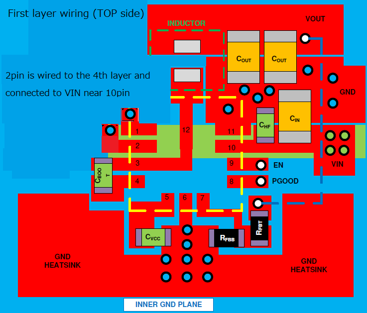
The layout is designed, but because the board area is small, the input capacitor uses one CHF (0.1uF) and one CIN (10uF).
The layout at that time is shown below.
The board I design has four layers. The second and third layers are ground.
CHF should be placed near 10pin. No CHF is placed on 2pin and only the wiring is connected to VIN on the 4-layer side.
Is there any problem when doing the above layout?
Best regards,