This thread has been locked.

If you have a related question, please click the "Ask a related question" button in the top right corner. The newly created question will be automatically linked to this question.

TPS650864: TPS6508640RSKT: no default output for LDO5P0 & LDO3P3

Part Number: TPS650864
Other Parts Discussed in Thread: IPG-UI, USB2ANY

Dear,

In order to evaluate the TPS6508640RSKT to power the Xilinx MPSoC ZU9, we have designed a power board which only contains TPS6508640RSKT and the required components.

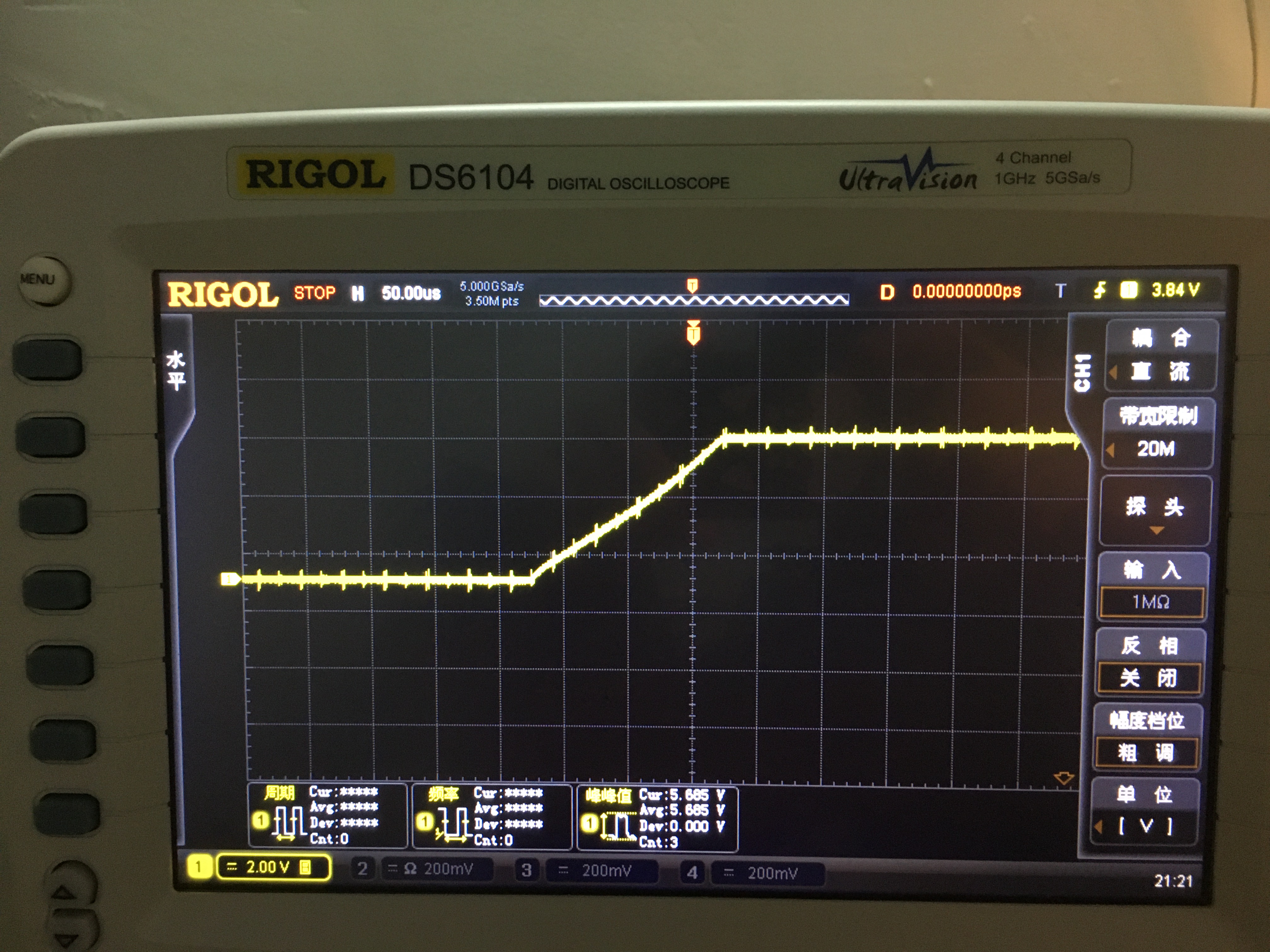
In the initial test, with the input power supply being12V and all the load's being off, we found that LDO5P0 and LDO3P3 do not have output voltage. In my understanding, as long as providing with 12V power, LDO5P0  and LDO3P3  should give the appropriate output voltage. Is my understanding correct? Or any other reason to cause TPS6508640RSKT shutdown?

Thanks ahead.

Regards,


  • Hello,

    Yes, in general as long as VSYS > 4V, LDO3P3 should be always present. The only thing that I know as gating that is VREF stability. Have you probed VREF?

  • Hi  Kevin,

    We get two boards at hand, one is like what I posted, it does not give the LDO5P0 and LDO3P3 output and the VREF is 0 voltage. Need further debug.

    For the other board, it has LDO3P3 output with VREF being 1.25V, which I think correct, right? But LDO5P0 gives nothing out, and the chip is quite hot.

    In the normal operation without any loads, how much is the estimated power consumption? For my situation, the power cost is  3.6W(12V * 0.3A). Could you give some advice to further debug the LDO5P0?

    Thanks.

    Chunjie 

  • Hi Chunjie,

    The first case sounds most likely to be either soldering issue or ESD damage. There is no case where VREF will not be enabled by PMIC. 

    The second case is less clear. 300 mA sounds like the LDO5P0 currently limit is being hit, can you check if it is shorted to GND?

    Can you help to provide the schematic as well?

  • Hi Kevin

    Attached is the schematic about TPS650864, please have a check.

    I will continue the debug and the latest result will be updated ASAP.

    Regards,

    Chunjie

  • Hi Kevin,

    When the input is beyond 5.7V, LDO5P0 starts to give output about 1.8V, and as with the input increasing, LDO5P0 still keeps at 1.8V output. During this process, the VREF stays at 1.25V and LDO3P3 stays at 3.3V.

    When checking the schematic, it is found that SWB1 and SWB2 are connected together, shown as the last post, is it OKay?

    Regards,

    Chunjie

  • Hi Chunjie,

    Did you check the resistance from LDO5P0 output to GND on your board when no power is applied to the system? 

    With LDO5P0 measuring 1.8V I see two possibilities:

    1. There is a ~9 Ω short to GND on LDO5P0 pin on your board. The current limit has a 200 mA limit (probably typically closer to 300 mA), so 1.8 V / 200 mA = 9 Ω. 

    2. Input supply is unstable. To test this, please provide an oscilloscope shot of VSYS pin (C1096) and LDO5P0 output (C1098). If VSYS is crashing below 5.7 V during start-up then LDO5P0 would be turning off and on cyclically which could give a measurement of 1.8V DC if it is oscillating between 0 and 5V

    From schematic, having SWB1 and SWB2 shorted together would lead to some power loss (the voltage on SWB1 output will discharge some current through the SWB2 discharge resistor), but I would not expect any other issue.

    What is controlling the TPS6508640_PG_CTL4? Just want to confirm that it is going high after GPO1. Otherwise BUCK2 and BUCK1 will turn on at the same time.

  • Hi  Keven,

    Following your advice, we check the resistance from LDO5PO to GND, it's about  2KΩ, which should be okay, I think.

    For the input supply, it is stable and not crashing during the start-up.

    Finally, we made a trivial and cut the PCB routing from LDO5P0 to DRV5V_2_A1/DRV5V_1_6, and get the LDO5P0 output at 4.95V. Amazing!

    We check the schematic and PCB layout, no potential issues are found.

    According to the datasheet, it is recommended to shorten the DRV5V_2_A1 and DRV5V_1_6 to GND by a 2.2uF cap, but we use 10uF, is it Okay?

    Regards,

    Chunjie

  • Hi Chunjie,

    I would not expect 2x10uF capacitors to create an issue compared to 2x2.2uF. Can you provide scope shots of LDO5P0 during start-up? You could try reducing to 2.2uF and see if it improves.

  • Hi Kevin,

    As you said, there is no improvement when replacing 2x10uF with 2x2.2uF.

    I captured LDO5P0 and CTL4 shots during the start-up, of which both seem okay. CTL4 is the PGOOD signal of another DC-DC chip TPS544C25RVFR

    Regards,

    Chunjie

  • Hi Chunjie,

    Are these scope shots with the DRV5V_2_A1 and DRV5V_1_6 connections to LDO5P0 cut? I was hoping to see the case where LDO5P0 measured as 1.8V.

    However, I had another thought today; if measured resistance when off is high, then it suggests that maybe one of the outputs of the BUCK1/2/6 driver could be shorted to GND? When you disconnect those pins, the LDO5P0 boots fine, but I'm assuming the BUCK1/2/6 don't power up as expected?

  • Hi Kevin

    In the last post, the scope shots are made when DRV5V_2_A1 and DRV5V_1_6 are cut off from the LDO5P0.

    For your idea about BUCK1/26 drivers being shorted to GND, it's okay in my test. When DRV5V_2_A1 and DRV5V_1_6 are disconnected from LDO5P0, BUCK1/2/6 is not working as expected.

    The attached scope shot shows that when both of DRV5V_2_A1 and DRV5V_1_6 are shortened to LDO5P0 during start-up.

    I also did another trivial that cut off the connection between DRV5V_2_A1 and DRV5V_1_6, so that either could be shortened to the LDO5PO. Under such a circumstance, the LDO5P0 is 2.1V.

    At this point, could we guess the current is not enough so that LDO5P0 is dropped down?  Just a guess since the trace from DRV5V_2_A1/DRV5V_1_6 to LDO5P0 point on PCB is above 8 mils, which I think should be okay.

    Regards

    Chunjie

  • Hi Chunjie,

    Given that you mentioned that the current going in was 0.3A, which aligns with the LDO5P0 current limit, I still think we are looking for a short.

    To confirm, you found that LDO5P0 had only 2.1 V output when shorted to DRV5V_2_A1 but not DRV5V_1_6? Also LDO5P0 had only 2.1 V output when shorted to DRV5V_1_6 but not DRV5V_2_A1? That is how I interpreted: "I also did another trivial that cut off the connection between DRV5V_2_A1 and DRV5V_1_6, so that either could be shortened to the LDO5PO. Under such a circumstance, the LDO5P0 is 2.1V." Please let me know if that is not what you did.

    I should have been more clear; regarding the short that I mean to look for is not on the DRV5V_x_x pins, but on the output of the driver. So, BOOTx, DRVHx, SWx, DRVLx, FBVOUTx, PGNDSNSx, or ILIMx. If one of these is shorted, the DRV5V_x_x would measure high resistance when OFF, but would have issues when the PMIC is enabled. Also, can you check BOOTx to DRVHx and DRVHx to SWx since a short on these would also cause excess current draw.

    If you confirm that none of these seem to be shorted, then I think next step is to try to replace the PMIC and see if the failure systems remain the same. Do you have any boards that are working as expected?

  • Hi  Kevin,

    For the question that you wan to confirm, your understanding is correct.  DRV5V_2_A1 and DRV5V_1_6 are shorted to LDO5P0 individually.

    For the issues about short, it's found that DRVL6 is shorted to PGNDSNS6. Oh, my god. Another sodering issue, which would kill me:). But the reality is that I cannot separate them, how about cutting the 12V supply off?

    Sadly, I only have one board work and there is no way to make cross-check.

    Many thanks for your professional answer again. Quite helpful. 

    Regards,

    Chunjie

  • Hi Chunjie,

    DRVL6 short to PGNDSNS6 does explain why LDO5P0 short to DRV5V_1_6 would cause LDO5P0 output to fail; when the device powers up it was try to charge the DRVL circuitry and fail. It also explains the 300 mA current draw.

    With DRVL shorted to GND, I'm not sure the total implications. I suspect you could leave LDO5P0 disconnected from DRV5V_1_6 and power up the PMIC as long you did not enable BUCK1 or BUCK6. You could test BUCK3/4/5 for example by forcing all the CTLx pins low and then enabling them by I2C using a USB2ANY box + the IPG-UI.

    Let me know if I can help in any other way.