This thread has been locked.

If you have a related question, please click the "Ask a related question" button in the top right corner. The newly created question will be automatically linked to this question.

UCC21530: I'm having trouble simulating the output of the gate driver on Tina TI

Part Number: UCC21530

hi,

i have asked the same question in my previous discussions,please do not get annoyed :D

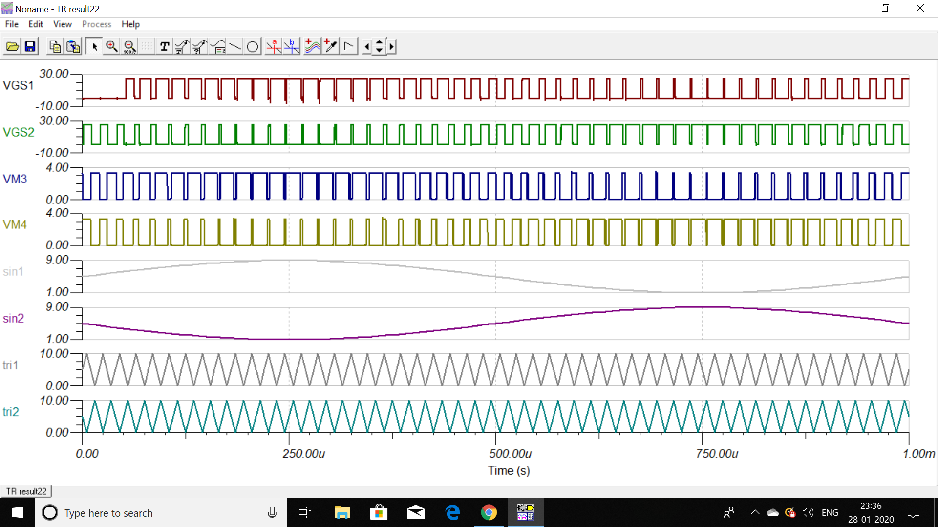
I tried to simulate the gate driver circuit along with the power mosfets(SCT3040kl),now the problem i am facing is gate to source voltage of the T2 is desirable output but gate to source voltage across the T1 is bit strange,please look into it and i am attaching the circuit file and screen shot of the output waveforms.

A quick reply would be appreciable.

Thanking you.

model_test.TSC   

  • Hi Vempuluru,

    These waveforms look pretty typical to me for a high voltage half-bridge circuit. Can you please point out what you find a bit strange?

    Thanks and best regards,

    John

  • actually VGS1 should follow vm3 instead it is being low for sometime and then it is following but vgs2 the output is desirable.

  • The missing high-side pulses at the start of switching is expected due to the bootstrap circuit only providing power to the high-side after the low-side has started switching. The typical UVLO power-up delay for this device is approximately 50us, as found in section 7.5 of the UCC21530 datasheet.

    If the system can not tolerate the missing pulses, we typically recommend using an isolated power supply for the high-side driver, or running a bootstrap pre-charge routine which charges up the bootstrap capacitor with a couple short low-side pulses.

    If this answered your question, could you please press the green button? If not, feel free to ask more questions.

    Thanks and best regards,

    John