This thread has been locked.

If you have a related question, please click the "Ask a related question" button in the top right corner. The newly created question will be automatically linked to this question.

LM5165: LM5165X output oscillation problem

Expert 6310 points
Part Number: LM5165

Team,

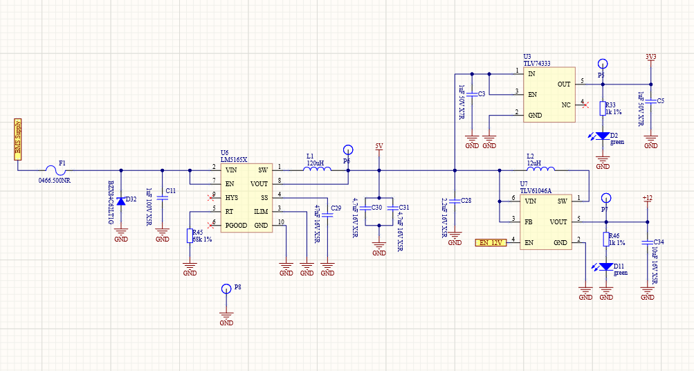
we use LM5165X to convert 48V from battery to 5V, in general it works fine, though when measuring the voltage on the battery with a multimeter, we see a voltage oscillation going to the output of the converter. This oscillation causes a reset of the MCU (5v powered). 

What is the best way to address/minimize this oscillation (ferrite bead, additional caps, common mode choke)? 

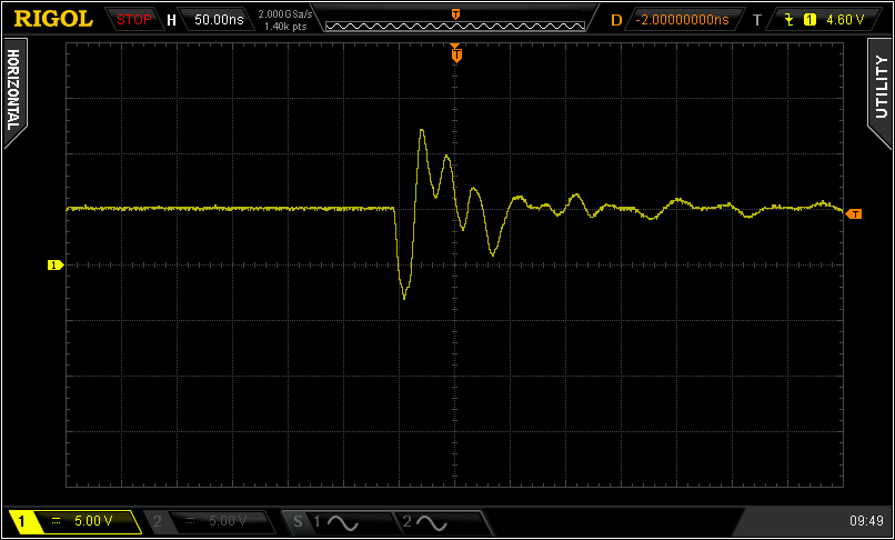
The first scopeshot is when on batt. power, the second on 5V. Oscillation lasts a few tens of nanoseconds, but it's enough for the MCU. Voltage on the battery 41.2V oscillates max to 75.2V and 34V.

Thank you.

  • Bart,

    The most likely case is that the input capacitor is not close enough to the IC. That loop inductance causes a ring when the device switches. Larger loop inductance means larger ring. Move the cap so that it has the smallest loop area from VIN (pin of IC) through the cap to GND (pin of IC).

    If that does not help, or if the cap is as close as possible already, please share the layout.

    -Sam

  • Hi Sam,

    thanks for your feedback. We tried to put the cap really close to the converter. Please find the layout in your mailbox.

    Thank you.

  • Bart,

    The layout shows a small trace connecting the VIN plane to the VIN pin of the IC. This will add inductance and increase this ringing.

    A bigger issue is that the SW pin of the IC goes into a thin trace, through a via to the bottom layer, through a long thin trace, through another via to the inductor. This long thin trace has inductance which will ring with the interwinding capacitance of the inductor causing noise on the output.

    Another issue is that the output capacitors do not have a clear path back to the GND pin of the IC or the GND pad of the CIN cap. This also increases the loop area and loop inductance.

    -Sam

  • Sam,

    thanks for your feedback, we will adjust the layout based on that.

    Question regarding your point about the trace of SW pin - we were doing it based on http://www.ti.com/lit/ug/snvu474/snvu474.pdf, pages 20-21. Do you suggest that this might not be optimal layout?

  • Bart,

    SNVU575 is titled a "High density EVM" meaning the board is very small to demonstrate a small solution size. This comes with some sacrifices. The component placement is limited by the space so the parasitics are not minimized (at least in the case of the SW node). The layout you shared appears to have more space which would allow for more optimal component placement.

    The datasheet has layout recommendations in section 10.1

    -Sam