This thread has been locked.

If you have a related question, please click the "Ask a related question" button in the top right corner. The newly created question will be automatically linked to this question.

TPS22919: Short-circuit protection kicks in at 0.7 A

Part Number: TPS22919
Other Parts Discussed in Thread: TPS22963C,

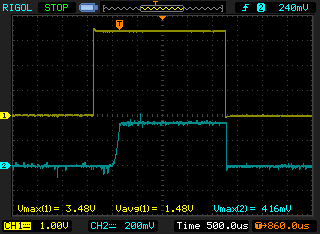
I want to switch a purely resistive load, and thought TPS22919 would be a good choice. The over-current protection is specified to start at around 3A. However, in my circuit I can't get more current than 0.7 A before the TPS22919 starts absorbing the effect, outputting only around 0.12 A.

I control TPS22919 with 3.3 V logics and an external 20 Kohm pulldown to ground

I need 1-1.5 A, from a 3-4 V power source, to heat a hot wire for very short lengths of time. This means I will use a load of 2.5-4 ohm.

Is this within specs for TPS22919?

Could the small load resistance or the small ground potential generated by the return current trigger the over-current protection? Any other potential reasons?

Can you suggest an alternative IC/circuit of similar size, ideally with current limit around 1.5 A instead of shutting off the output?

Thanks in advance

  • Anders,

    You are almost certainly hitting thermal shutdown in this scenario. Keep in mind that the on resistance changes with temperature. With a worst case scenario of a 125C ambient temperature we have an on resistance of 250mΩ (at 3.6V which is a good midpoint at the range you specified) you will have a power dissipated of 563mW. Multiplying it by RθJA and adding it to an ambient temperature of 105C (the max) we get a junction temperature 224C which is well above the device max. Even if you do the power calculations at more conservative temperatures/voltages you are still exceeding the max junction temperature. 

    Your better bet here would be a device with a lower on-resistance that has a little bit more wiggle room for the current you are trying to drive. The TPS22963C http://www.ti.com/lit/ds/symlink/tps22963c.pdf would be able to fit your needs. At your numbers you would be getting a max junction temperature of 113C which is well below the 125C max. 

  • Thanks for your reply, however this can not be the explanation. I test at ambient temperature 25 C. If this was thermal shutdown, the current should rise when the IC is enabled, then fall back as the IC heats up. I don't see any initial current spike, even for a microsecond. A thermal camera confirms there's no heating when I run for a few milliseconds. I think any internal runaway heating would have to be so local and immediate as to invalidate the specs in all scenarios.

    If I do the calculation at 25 C ambient, the typical on-state resistance is 90 mOhm meaning 1 A would produce 0.09 W and 18.9 C heating. 1.5 A should give 0.2 W and 42 C heating. This should provide a margin, but even 0.7 A does not work. And the IC will never be active for more than a second anyway.
    There's a clear limit around 5 ohm load. Any larger load resistance works fine. Any smaller, and the output voltage curve looks as in datasheet figure 23 "Turn on into an output short", capping the output voltage sharply 200 us into the rise without overshoot, to around 0.15-0.3 V.
    There's no indication of disturbance on either VIN, VOUT or ON.
    The IC shares ground with the current return path at a via, but diverting the return current makes no difference. Adding a 4.7 uF cap on VIN didn't change anything. Soldering another TPS22919 only changes the limit to around 0.8 A (4 ohm at 4 V, plus other circuit resistance). I have tested two different PCBs and two locations on the PCB. No difference with different power sources. I've exhausted all ideas.
    TPS22963C is unfortunately four times as expensive, has a higher shutdown current and would be harder to route.
  • Anders,

    Apologies for the misfire here on the thermal shutdown. I did read your question wrong. In your case if you are testing at an ambient temperature of 25C then you definitely should not be hitting thermal shutdown and the problem here is likely something else. Just do keep in mind that if in your system you plan on going higher in ambient temperatures then the higher current profile might potentially run into heating issues.

    What would be helpful here to diagnose the issue would be a (partial) schematic on how the TPS22919 is connected. How is your QOD pin setup? Are there any major capacitances on the load side? A scope shot (with a current probe preferably) would be useful here too to dig into the details.  Essentially we just need to look at the TPS22919 when it is on as a resistor with a resistance of Ron. If it is indeed triggering on the short circuit detection then the voltage drop across that resistor has to be over the trigger voltage drop (VSC in the datasheet) so a scope shot should help bring some of this to light. 

  • Thanks

    Here's a sketch of the schematics.

    CURRENT_SENSE goes to MCU ADC. I try with different values for R1.

    R4 and R5 roughly corresponds to my measurements of real-world conditions.

    I show scope shots with VBAT=5V, R1=3.1 ohm and R2=1 ohm. Lower R1+R2 gives the correct (working) VOUT ~= VIN. Doing a more direct current probe would be some work, given the realities of the PCB.

    yellow=VIN, blue=VOUT:

    yellow=ON, blue=VOUT:

    yellow=CURRENT_SENSE (R2 ~= 0.8 ohm), blue=VOUT 

    Zooming into the CURRENT_SENSE shot doesn't reveal any further details.

  • Anders,

    Sorry for the delayed response here. Just judging by the scope shots and the schematic there does not appear to be anything that appears wrong here. I am going to take the TPS22919EVM into the lab to reproduce your setup here just as a sanity test. I will have results within a day or so. 

  • Thanks for looking into this.

    I can brainstorm three areas where the IC may be sensitive from deviations from the reference design: decoupling, resistance/inductance in power supply, and sensitivity from EM fields from the current itself.

    (And capacitive loads, but that's not the case for me.)

    Any such pitfall would be helpful for me and other users to know about as the effect is a non-functional circuit, not just degraded function.

  • Hi Anders,

    Thank you for the information and scope shots, it makes looking into this problem much easier :). I believe I know what may be happening based on your implementation of the device.

    Overall, the device has two current limits, one at ~3A and another at ~500mA. When the device first turns on, it uses the lower current limit setting until it reaches ~0.36V, and then the 3A current limit is activated. The reason the device starts up this way is because it keeps the device protected when turning on into a short, and the beginning of turn on is when the most amount of power is being dissipated. If the device is continuing to hit the current limit after it reaches 0.36V, then it will keep the voltage there and continue holding the current until the perceived short is removed. With an IC as a load, this is not an issue since an IC would have UVLO and not pull current until VOUT is much higher than 0.36V. With a pure resistive load, current is always being pulled, so the device won't be able to turn on. I believe this is what is happening with your device based on the measure VOUT voltage and current you are trying to pull.

    Are you able to turn on the device without the load and then apply the resistive load after turn on? I think this would prove out the speculation above.

    Thanks,

    Alek Kaknevicius

  • Hi Alek

    Indeed, connecting the load some time after the switch is turned on changes the behavior and allows more current. I haven't verified exactly how much current.

    Your analysis is probably correct, meaning the IC is not suitable for my application as I need to drive a load with constant resistance.

    It might be helpful for future users if you can amend the TPS22919 datasheet to mention this stricter limit during the startup sequence.

    Best regards