This thread has been locked.

If you have a related question, please click the "Ask a related question" button in the top right corner. The newly created question will be automatically linked to this question.

TPS7B7702-Q1: How can I calculate Rds(on) of FET in LDO?

Part Number: TPS7B7702-Q1

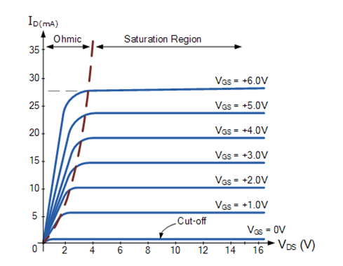
I have some questions regarding the internal FET operation of LDO.

1. In LDO, which uses pass device as FET, Rds(on) is dominated by Vds rather than Vds, Id. Is this right?

2. Assuming Vin=14V, Vout=5V, Iload=100mA, is it Vds=9V and therefore Rds(on)=90ohm?
Assuming Vin=40V, Vout=5V, Iload=100mA, is it Vds=35V and therefore Rds(on)=350ohm?

3. So, is the Vgs adjusted to make Rds(on)=90, 350ohm via feedback?

Does it have to be a specific Vgs to satisfy certain Iload in certain Vds? (and value of Vgs define by FET characteristic)
-------------------------------------------------------------------------------------------------------------------------------------------------------------------------------------------------------

If above 1~3 is correct,

1. At TSP7b7702 datasheet, max Vdropout at Io=100mA is 500mV which means that Rds(on) is among 5ohm(500mV/100mA) and it seems too big compared to typical low Rds(on) FETs. Can't smaller Rds(on) of FET to lower Vdropout? Why is it used so high?

  • Hi Hyeon,

    The best way to estimate the effective RDSON is from the VDO specification in the datasheet:

    So when the FET is fully enhanced the RDSON is ~5Ohm.

    When an LDO is in regulation, it is working in the triode region so the FET is not normally fully saturated. So your calculations above are essentially correct for that operating condition. To answer your questions:

    1. In LDO, which uses pass device as FET, Rds(on) is dominated by Vds rather than Vds, Id. Is this right? *The LDO modulates VGS to ensure that the output voltage is in regulation. Meaning if the input voltage moves up and down(i.e. VDS is changing), the VGS of the FET is modulated to regulate VOUT. This is also true if the load current (IDS) changes. To see how well the LDO does this, look at the line regulation and load regulation specifications. 

    2. Assuming Vin=14V, Vout=5V, Iload=100mA, is it Vds=9V and therefore Rds(on)=90ohm?
    Assuming Vin=40V, Vout=5V, Iload=100mA, is it Vds=35V and therefore Rds(on)=350ohm? *Yes at this specific operating point these statements are true. 

    3. So, is the Vgs adjusted to make Rds(on)=90, 350ohm via feedback? *Yes. the VGS is modulated based on VDS and IDS to ensure V is well regulated. 

    Does it have to be a specific Vgs to satisfy certain Iload in certain Vds? (and value of Vgs define by FET characteristic)* Yes, this is how all Linear regulators work. 


    I hope this helps to clarify.

  • Thank you for your kind answer!

    But I have an additional question.

    1. You told me LDO is working in the triode region and as far as I know, the area should be in Vds<=(Vgs-Vth).

    Assuming Vin=14V, Vout=5V, Iload=100mA, and Vgs=8.27V. Isn't it Vds=9V, Vgs=3.27V witch means it's in saturation region?

    2. Aren't Vgs-Id, VDS-Id graphs provided by FET datasheet the data corresponding to the saturation area? (Of course, the trial region is shown in Vds-Id.)

    Is there a way to match the correlation between Rds(on), Vgs, Vds and Id in the two graphs above?

  • Hi Hyeon,

    You're welcome. 

    For Question #1. How are you arriving at VGS=3.27V? This is driven internally to ensure that VOUT is properly regulated.  The FET is only in saturation when VIN-VOUT<=VDO

    For Question #2. The difference between an LDO and a FET is that you can not directly control the VGS of an LDO. I think you are looking at how ID is modeled in an ideal FET:

    ID=unCOX*(W/L)*((VGS-VTH)VGS-VDS^2/2)

    This is a model for the drain current in any FET. 

    Since we do not bring the gate drive external to the IC, it is not possible to make the curves that a FET can. We are doing a few things a single FET does not:

    1. Our primary focus is to regulate an output voltage. 

    2. We also limit the maximum current (either through brick-wall or fold-back current limit depending on the LDO).

    3. We have thermal protection. 

    I hope this helps.

    Regards,

  • Thank you very much for your reply. Those are probably the last questions.


    1. Assuming Vsupply=Vin=12V, Vout=5V, Iload=100mA

    It means Vds=7V(Vin-Vout), Vs=5V(Vout) requires higher Vg than 12V in order to operate in a tripode region (Vds<Vgs-Vth & Vgs=Vg-Vs). Then, required FET gate voltage is greater than Vsupply, and I don't know how this is formed.

    2. The graph on the left is a graph that can be obtained by searching 'N-type MOSFET Characters Curves' and the graph on the right is a graph commonly used in 'LDO dropout documents'. Are the two meanings different?

  • Reuplod two graphs


           'N-type MOSFET Characters Curves'   

                              'LDO dropout documents'

  • Hi Hyeon,

    For question #1: with VIN=12V and VOUT equals 5V, The LDO has more than enough headroom to properly drive the gate, In the N-Channel case, we need a rail ~1.5-2V above the Source in this case VOUT. In the P-Channel case, we need ~1.5-2V below VOUT to properly drive the gate. We can create both bias rails internally. An easy way to see this is when looking at a simple P-Channel datasheets VDO:

    Here is a VDO chart from the TLV767:

    The Arrow is showing the region where the FET is exited saturation and entering into the triode region.

    For question 2: The chart you show for the transition between the Ohmic (triode) and Saturation region for the MOSFET characterization curve is more correct. the 2nd graph you show for LDO's is more idealized. During normal operation, the LDO is always operating in the Ohmic or Triode region. Only when VIN-VOUT is equal to or less than the VDO does it enter into the saturation region. 

    I hope this helps to clarify.