This thread has been locked.

If you have a related question, please click the "Ask a related question" button in the top right corner. The newly created question will be automatically linked to this question.

UCC5350: UCC5350: UCC5350MC schematic with only one +15V power supply

Part Number: UCC5350

Good morning, sir,

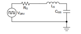
I want to use the UCC5350MC with the Miller clamp. Is it possible to use the same power supply for Vcc1 and Vcc2 (+15V 1A) ? I have only one power supply available.

Is it possible to make the system exactly as in the following item (https://e2e.ti.com/support/power-management/f/196/t/810262?tisearch=e2e-sitesearch&keymatch=UCC5350) by simply replacing the -3V by a GND?

Thank you in advance,

Best regards,

Maxime


  • Hi, Maxime,

    You can only do this if GND1 is the same potential as VEE2. If those two pins aren't at the same potential, then you need to use some kind of isolated power supply technique on the output side.

    If this answered your question, please press the Green button. If you have more questions, please let us know!

  • Yes thank you very much, the idea is to isolate only the IN+ signal.

    Another small question, in the case of the "S" version, how to define the value of the output resistors Rgon and Rgoff?

    Thanks again,

    Maxime

  • Maxime,

    The external gate drive resistors R_gon and R_goff are selected such as to minimize ringing from parasitic inductance and the input Capacitance of your IGBT.

    This Tech Note describes an iterative process to size the external gate resistors with a goal of reducing ringing on the gate node.
    www.ti.com/.../slla385.pdf


    To follow this process, you only need to know a few things: 1) Input capacitance (C_ies) from the IGBT datasheet, and 2) you will need to measure the ringing frequency (f_r) with R_gon=R_goff=0 Ohms. Then, you can calculate the parasitic inductance based on the resonant frequency of ringing after an edge, and calculate Rg based on a selected quality factor (to create either critically damped or underdamped system) to build a system like in the diagram. It’s essentially a compromise between reducing the unwanted oscillation and a slow rise time. You should start with critically damped and move towards an underdamped system for these calculations if you’re getting unacceptably slow rise times.

    user5962098 said:

    the idea is to isolate only the IN+ signal.

    I am not sure what you mean by this, but it shouldn't change my response regarding gate resistor sizing.

    Could you elaborate on what you mean by isolating only IN+? Are you referring to only using IN+ and grounding the inverting input?


    If I've answered your question, please click on the green button. And do let us know if you have follow up questions.

    Best

    Dimitri James


  • Hi,

    Exactly, I'll just use the IN+ input and ground the inverted input.

    My final application is driving a mosfet transistor for periodic pulses on a power led. The command comes from an FPGA output.

    I don't think I need the Rg resistors.

    Thanks,

    Maxime