This thread has been locked.

If you have a related question, please click the "Ask a related question" button in the top right corner. The newly created question will be automatically linked to this question.

CSD16325Q5: CSD16325Q5

Part Number: CSD16325Q5
Other Parts Discussed in Thread: CSD17573Q5B

Hi,

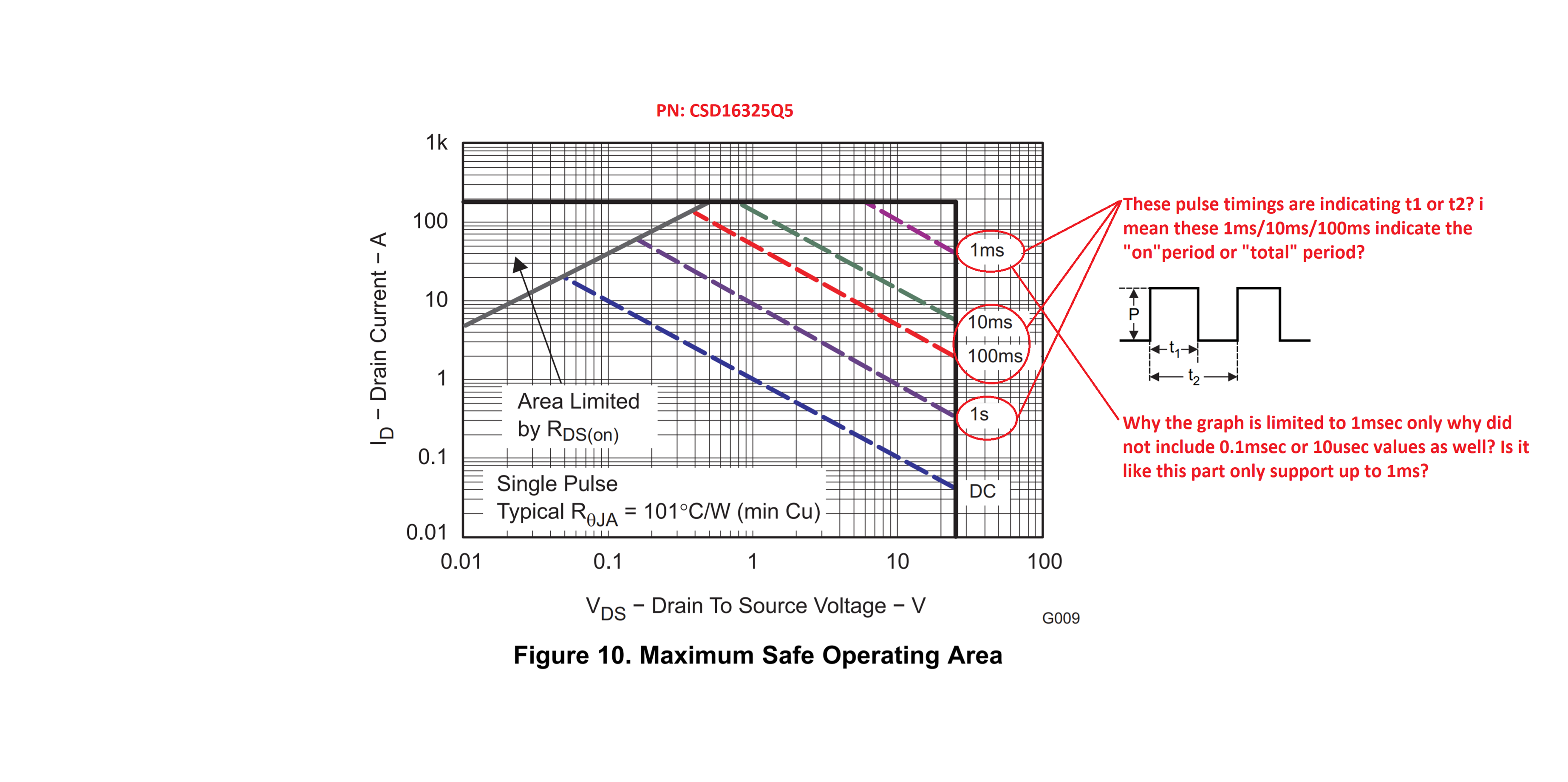
Please see image below, the pulse timings mentioned in the SOA graph, are they the "on" timings of the pulse or "on+off" timings?

I mean if say 1msec means a pulse with 1msec "on" period or a pulse with 1msec of "total" (on+off) period? if 1msec is total period then what is the on period or duty cycle for 1msec? How to understand these numbers?

Also why the graph shows pulse width only up to 1msec why not 100usec or 10usec and further? Does this mean this MOSFET can only support pulses of 1msec not faster/smaller pulse widths than 1msec?

Please suggest

Thanks

Santosh

  • Hi Santosh,

    Thanks for your interest in TI FETs. Below you will find a link for how TI specifies SOA in our MOSFET datasheets. The SOA curves included in the CSD16325Q5 datasheet are for a single on pulse. For repetitive pulses, you can use the transient thermal impedance curves included in the MOSFET datasheet. The CSD16325Q5 is an older device and the SOA curves are calculated. For pulse widths < 1ms, the maximum current is limited by the absolute maximum current ratings (200A) on page 1 of the datasheet. Because this is an older device, we recommend the CSD17573Q5B as a newer replacement. This SOA curves in the datasheet for this device are based on actual test-to-failure data.

  • Hi John,

    Thanks for the reply.

    referring CSD17573Q5B datasheet it is mentioned in the 1st page a continuous drain current of 43A. Does this mean I can pull 43A continuously if I have a heatsink that can maintain TJ below 150degree Celcius?

    TJ =130 (derated)

    TA = 40

    Pd = 43A(ID) *1V(VDS) = 43watts

    TJ= TA + Pd * Rth(JA)

    130=40+43*Rth(JA)

    Rth(JA)= 2 degree/watt

    So if I choose a heatsink (active/passive) with thermal resistance 2 or less than 2 degrees Celcius per watt will I be able to pull a continuous 43A drain current with VDD at 1V? Is my understanding correct?

    Please suggest

    my circuit below

  • Hi Santosh,

    The continuous drain current ratings on page 1 of the MOSFET datasheet are calculated quantities except for the package limited current which is determined by the interface between the silicon die and package/lead frame. This can either be bond wires or copper clip which the CSD17573Q5B uses. I've included some links below that explain continuous current ratings, thermal impedance and power dissipation capability by package for TI FETs. Your calculation is correct. However, achieving RthetaJA of 2degC/W is going to be very difficult if not impossible to implement. TI specs RthetaJC to the thermal pad on the bottom of the package at 0.8degC/W max. Dissipating 43W continuously in a 5x6mm SON package is not practical. If this is pulsed, you can use the transient thermal impedance curves in the MOSFET datasheet to calculate the junction temperature rise. You may want to consider paralleling multiple FETs to spread the heat over a larger surface area and number of packages.

  • Hi john

    yes, eventually I will parallel the MOSFETs. But my main concern is how much max current can I pull from a single MOSFET practically.

    Practically in the sense with practical Rth(JA). Not like Tcase as 25degC. I am assuming Tcase to be 75 to 100degC

    So please suggest what is the maximum continuous drain current practically I can pull through a single MOSFET(CSD17573Q5B) with VDS as 1V. 

    Also could you please suggest a MOSFET with Drain pad exposed on the top side instead of the bottom so that I could have a heatsink attached on MOSFET from the top. So that I can achieve 2degC/w heatsink

    Thanks

    Santosh

  • Hi Santosh,

    In theory, you can use the same calculation to determine the max continuous current at VDS = 1V as follows:

    PDmax = (Tj - Tcase)/RthetaJC, IDmax = PDmax/VDS

    For Tj = 130degC & Tcase = 75degC, PDmax = (130-75)/0.8 = 68.75W & IDmax = 68.75W/1V = 68.75A.

    In reality, you would need a heatsink and thermal interface that can dissipate 68.75W to ambient. If the ambient temperature is 25degC, then the required thermal impedance of the heatsink + thermal interface can be calculated as follows:

    RthetaCA = (75degC - 25degC)/68.75W = 0.727degC/W which is not very realistic for a SMT package where the main path for heat removal is into the PCB. You can heatsink the top of this package but RthetaJC to the top case is about 11degC/W. You can also heatsink the backside of the board. Without a heatsink, I have seen a good PCB design be able to achieve 20 - 25degC/W effective RthetaJA. Then the calculation becomes:

    PDmax = (Tj - Ta)/RthetaJA_eff = (130-25)/25 = 4.2W.

    At Ta = 55degC, this is reduced to 3W (IDmax = 3A at VDS = 1V).

    TI discontinued their dual-cool MOSFET packaged products with exposed metal on the top of a SON package. The only package TI offers that can be attached directly to a heatsink is the TO220. Below is a link to a listing of all TI FETs in TO220 package. RthetaJC for this package is 0.4degC/W max. There are many heatsink manufacturers that can help you with heatsink design and selection.

  • HI John

    Thanks for the explanations

    1) "RthetaJC to the top case is about 11degC/W"  how did you get this value?

    2) I understand continuous drain current 100A is limited by the package bond wires. If I try to pull more current than 100A the bond wire will melt is that correct? 

    3) Then what is the limiting factor for the pulsed current limit of 400A? How this number of 400A is figured out? Where is this limit coming from?

    Bcz for RDS(on) of 1.19mohm at VGS=4.5V(from datasheet) and VDD as 1V then ID=1/1.19mohm=840A

    4) What is the RDS(on) value for a VGS of 2.5V? bcz the VGS vs RDSon graph from datasheet shows only after 2.5V vgs

    Thanks

    Santosh

  • Hello Santosh,

    Thanks again for your interest in TI MOSFETs. Please see my answers below:

    1. Results from thermal simulations done by TI packaging team.
    2. The CSD17573Q5B and CSD16325Q5 are both copper clip packages. Instead of bond wires, the connection to the FET source uses a copper clip. 100A of current may not immediately melt or damage the copper clip but is the maximum current based on current density limitations.
    3. 400A is the maximum limit of TI's test equipment. IDM is a calculated value that uses the transient thermal impedance (Figure 1 in the datasheet) and assumes the case temperature is held at 25degC: PDM = (Tjmax - Tcase)/ZthetaJC & IDM = sqrt(PDM/rds_on), where the value for rds_on is at Tj = 150degC (about 1.7x the value at 25degC - see Figure 8 in the datasheet). Our calculation comes out to ~485A which is truncated down to 400A. Please check link to blog below.
    4. TI does not specify, test or guarantee rds(on) at VGS = 2.5V. The rds(on) vs. VGS curves included in the datasheet are for a typical device. VGS = 2.5V is on the very steep part of the curve where rds(on) increases exponentially. A slight shift in threshold voltage due to process variation can result in a large change in rds(on).

  • Hi John

    Based on the formulas you mentioned in point 3 and referring transient thermal impedance graph

    below are the PDM and IDM values at different pulses with a 1% duty cycle. In no case, i see IDM is 485 or 400 amps how did your calculations come ~480amps. Please suggests. Max ID is seen as 80A @10usec pulse with 1% duty cycle. I am confused.

    Pulse(1%Duty) Norm factor Zjc PDM IDM
    TJ 150 100msec 0.8 0.64 195.3 9.8
    TC 25 10msec 0.4 0.32 390.6 13.9
    Rjc 0.8 1msec 0.15 0.12 1041.7 22.7
    Rds_on 2.023 100usec 0.028 0.0224 5580.4 52.5
    10usec 0.012 0.0096 13020.8 80.2

    Also is there any minimum VDD required to pull a certain amount of ID. I mean, suppose I want to pull 40A @ 0.8 VDD is that possible? or do I need to have a minimum VDD above which only 40A ID is possible

    Thanks

    Santosh

  • Hello Santosh,

    I reviewed the IDM calculations for the CSD17578Q5B from the original characterization data. Below is how we arrived at 485A:

    • For 1% duty-cycle and 0.01s pulse width: normalizing factory = 0.375 (measured data)
    • PDM = (150C - 25C) / (0.8C/W x 0.375) = 417W
    • At 150C, rds(on) = 1.77mOhm (measured data)
    • IDM = sqrt(417W / 1.77mOhm) = 485A

    Now, I know the datasheet says that IDM is with pulse duration <= 100us and duty cycle <= 1%. I'm not certain why this calculation used ZthetaJC at 10ms pulse duration, 1% duty cycle. Obviously, the current would be much higher using ZthetaJC for 100us, 1% duty cycle. In any case, we truncate the value to 400A because that is the maximum current of our test equipment.

    I'm not sure what you mean by VDD. Should this be VDS, drain-source voltage of the FET? There is not a limitation on VDS to get 40A IDS. Please look at Figures 2 & 3 in the datasheet. With the right gate drive, you should easily achieve IDS = 40A at VDS = 0.8V. The typical data shows you will need VGS ~ 2.45 V to get IDS = 40A.

  • Hi John

    There was one mistake in my calculation for ID. I missed the "mili" in Rds_on. Below is the correct one and for 10msec 1%duty ID is ~453A. Which is fine since my Rds is 2.02mili yours is 1.77mili hence your ID is ~485.

    So if calculation is ~485A but because of your test equipment (you mean your power supply equipment is capable of 400A max), you are capping it to 400A right? SO it is not actually the MOSFET limit then. if you had a power supply with only 200A then you would have capped mosfet limit to 200A?

    And how did you measure Rds_on? please suggest


    by VDD I mean see attached image 


    Pulse(1%Duty) Norm factor Zjc PDM IDM
    TJ 150 100msec 0.8 0.64 195.3 310.7
    TC 25 10msec 0.375 0.3 416.7 453.8
    Rjc 0.8 1msec 0.15 0.12 1041.7 717.6
    Rds_on 0.002023 100usec 0.028 0.0224 5580.4 1660.9
    10usec 0.012 0.0096 13020.8 2537.0

    Thanks

    Santosh

  • Hello Santosh,

    As it has been explained to me, the 400A cutoff for IDM is a limitation of the equipment used to test TI FETs. I do not have any further details on this topic. TI tests rds(on) at the conditions specified in the Electrical Characteristics table in the MOSFET datasheet. The duration of the current pulse is very short (< 1ms) to avoid self-heating which would yield a higher value for rds(on) due to the positive temperature coefficient of that parameter. I am not at liberty to share any more information about TI's production test procedures.

  • Hi John

    Thanks for your support

    Appreciate your efforts

    Regards

    Santosh

  • Hi Santosh,

    You are welcome. Thanks again for your interest in TI MOSFETs. I think maybe we're getting too bogged down with the details in the MOSFET datasheet and not focusing on your application. To me, it appears that this circuit is used to test a DC-DC converter with a constant current load. Please let me know if I can provide any more insight or information as to how our FET will perform in this application.