This thread has been locked.

If you have a related question, please click the "Ask a related question" button in the top right corner. The newly created question will be automatically linked to this question.

TPS62051: VFB equals ~0.6-0.7V, SW pin not switching

Part Number: TPS62051

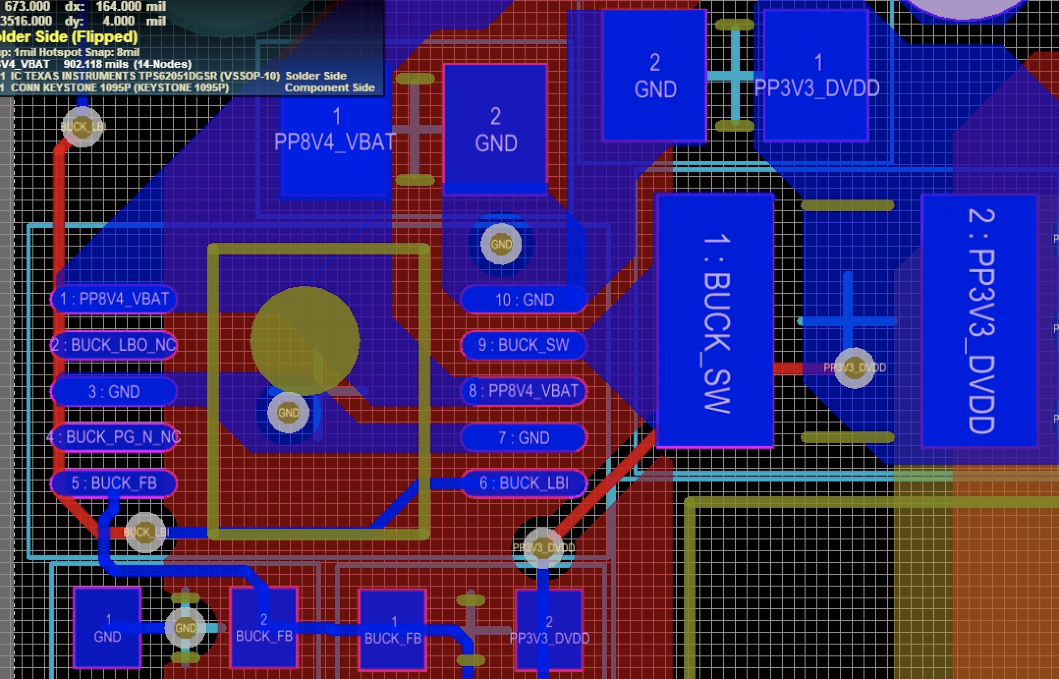
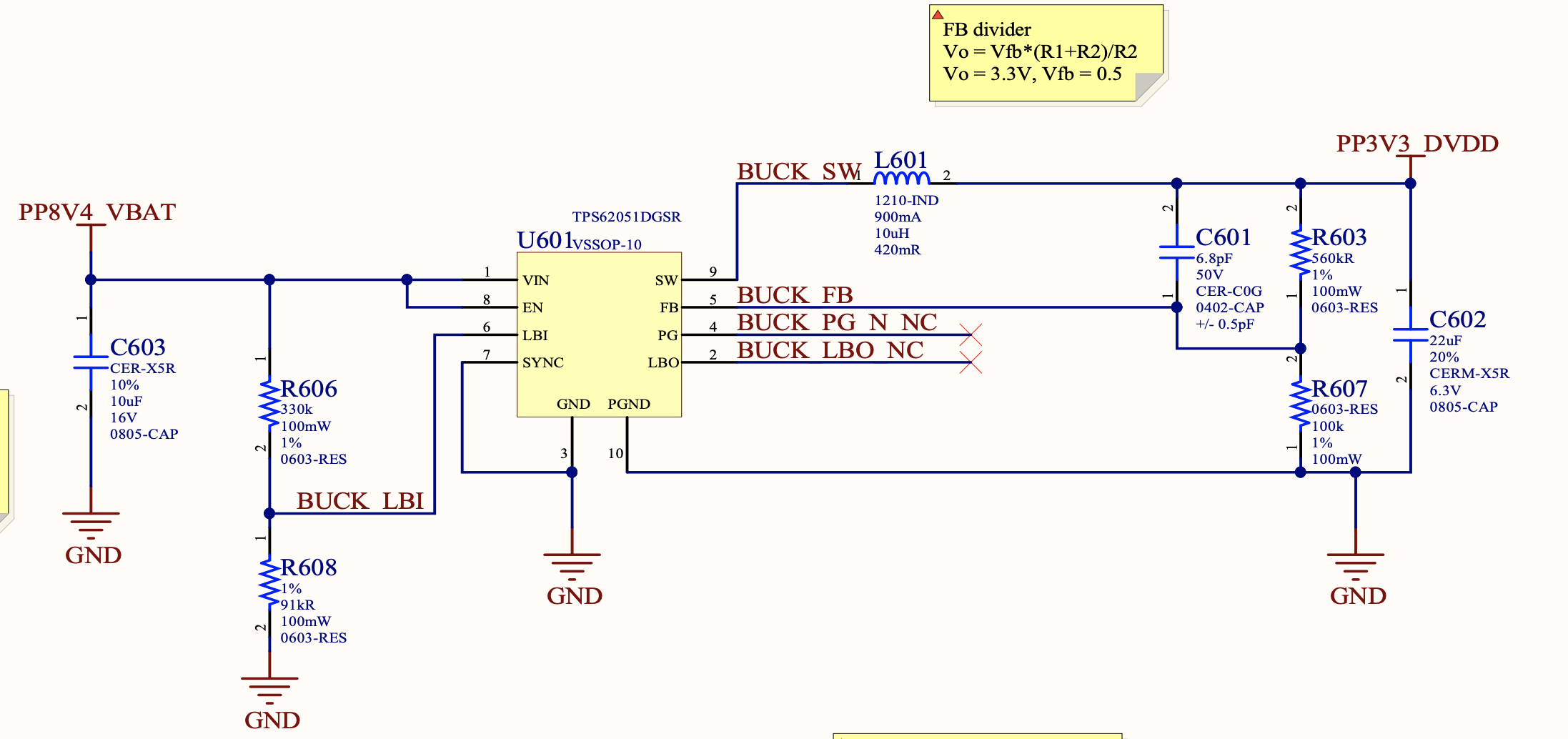
When powered on with 7.4V designed to step down to 3.3V (R1 = 560K, R2 = 100K), the part doesn't begin switching and the output follows the input linearly with Vin = 7.4V and Vout = 4.3V. The part may be broken but I wanted to check if this was an issue seen before. I have attached a picture of my layout (I used the reference design in Figure 6 of the datasheet). 

  • Jack,

    Layout looks similar to the datasheet. Need additional information on this.

    1. Can you please share actual schematic and BOM? 

    2. Any details of battery (chemistry and series/parallel cell counts) input used for this design and output current used for the testing?

    3. Please also share VIN, LBI and SW node waveforms. We want to ensure device is switching or not and also since TPS62051 has enhanced LBI, we want to ensure the voltage level is above the trip point. Please check page 9 section 9.3 of datasheet for LBI operation details.

    Regards,

    Amod

  • Hi Amod,

    Unfortunately it is difficult for me to measure all of those since I only have 1 probe. However, none of them are time-varying, and they are listed below:

    Vin: 7.5V

    Vout: 4.3V

    LBI: 1.51V

    SW: 4.3V (expected, not switching)

    Currently we are just using a power supply set at 7.5V to test this while we wait for the batteries to arrive. They are lithium-ion 18350s, 2S. The output current I did not control, since it is soldered onto my board. The schematic is attached. 

  • Hi Amod,

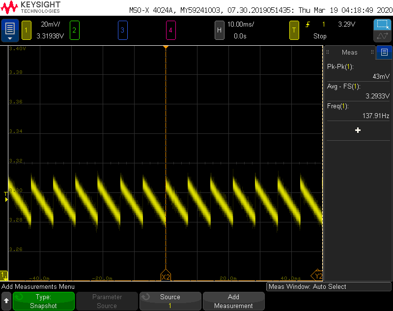
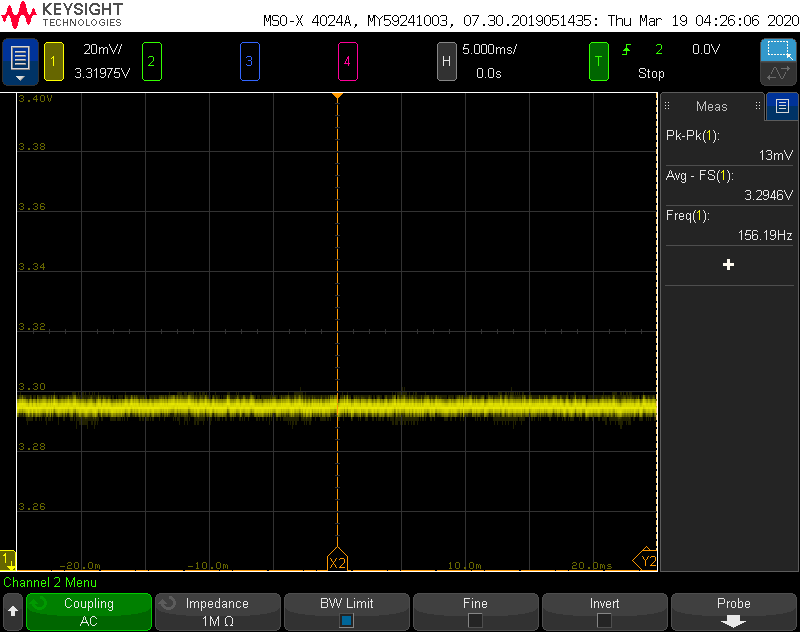
    Upon further investigation, the chip correctly starts up after LBI reaches 1.21V. However, when I increase Vin beyond ~6.41V, the chip then enters the behavior I described above, where the input follows the output linearly. After I increase Vin to 6.41V the output sits at 3.3V, then increases with the input from there. I have attached waveforms of the SW and Vout nodes during the correct operation and then after.

    During correct operation:

    After:

    Looking at these waveforms I see that in the first the converter seems to be bursting, since the frequency is about 140Hz, well below the specified switching frequency. The main load off of the 3.3V rail is an STM32L0 microcontroller. 

  • Hi Amod,

    So I discovered that at very low load (which is normal for the board), the converter exhibits this behavior of not switching after Vin exceeds 6.4V. However, when I attach a 1k or 10k resistor to the 3.3V rail, the converter works exactly as described and functions properly within the specified Vin range. I'm not sure why the converter would stop working at such low load, or if there is a different systemic issue altogether. 

    Jack

  • Hi Jack,

    Thank you for digging further into this and letting us know your findings.

    One thing I did not notice earlier was the R606 value needs to be 130kohm and R608 at 100kohm for the device to start working properly with LBI trip point > 1.21V at Vin>=2.7V. This may not be an issue necessarily depending on your input voltage but want to ensure the design can support lower voltages if required. With current resistor values (330k/91k), the trip point won't reach till ~5.6V Vin. Let me know if this is consistent with your testing results.

    I checked the device datasheet and found that when SYNC pin is LOW (like your design), the device should enter power save mode at low currents and should skip pulses and provide output regulation. I see only output voltage waveforms in your prior reply - is it possible to share switch node waveforms? We should see the skipping operation through these waveforms.

    Also, how much load current are you typically drawing from the microcontroller? I am not really sure at this point why adding a 1k or 10k resistor is helping with this situation as the device should be able to perform regulation in power save mode like I mentioned above.

    Regards,

    Amod

  • Hello Amod,

    Unfortunately we don't have the switching waveforms photos anymore and I won't have access to a scope for some time.  However, when the device is operating correctly (3.3V on the output) and the output current is sufficiently low (<100mA) our switching waveform behaves as explained in the datasheet: switching frequency is reduced and the device skips pulses as expected.  When the device is operating incorrectly (Vin > 6.4V) switching stops and only a DC voltage is observed at the switch node.  

    R606 and R608 voltages are correct for our application, we require a trip point of 5.6V.  This is consistent with our testing: the device starts operation at 5.6V until 6.4V when switching stops.  As we explained, if we attach a light load (10k or 1k from 3.3V to GND) the device operates correctly up to our Vmax of 8.4V.  

    Typical load for the microcontroller will vary, under sleep condition down to 0.23µA.  According to our device datasheet the maximum power draw will be 105mA.  Typical power draw depends on device operation but will be around 3mA.  

    I will continue investigating.   If you have any suggestions please let me know and I will check those areas.  Hopefully I can grab those scope screenshots for you soon but for now the descriptions will have to suffice. 

    Thank you,

    Robbie

  • Robbie,

    Thanks for the details! 

    No other suggestions but if you can share VIN, LBI and SW node waveforms

    1. when there is no external 1k or 10k resistor and Vin just lower than 6.4V when it is working properly and when Vin just greater than 6.4V when it stops working

    2. when there is external resistor and Vin just lower than 6.4V and when Vin just greater than 6.4V so we can compare these to waveforms in item 1 above.

    Regards,

    Amod