This thread has been locked.

If you have a related question, please click the "Ask a related question" button in the top right corner. The newly created question will be automatically linked to this question.

LMZM23600: Overheating

Part Number: LMZM23600

hello,

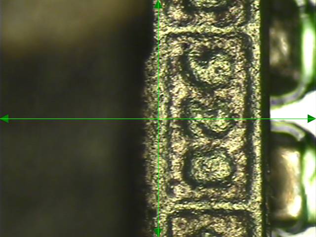
we have a similar phenomenon as Sasha Maldonado. We produced sample boards using the LMZM23600V5SILT. Schematic is per TI recommendation Figure 34 of data sheet SNVSB35B-February 2018, revised May 2019). We observe overheating on some of the boards. We had two proto production Batches: Batch 1:  6 Boards produced, whereas 2 of them are good, 4 with Overheating. As we had two good results, we excluded a General design error or PCB Layout error for the time being. We supposed maybe wrong/old solder paste and wrong stencil thickness. So we setup for a second small Prototyps Batch with 4 Boards: whereas 1 of them is good, three of them are overheating. After comparison and internal Analysis of all prototype boards from both Batches with good and bad results we still assume that we have Problems in the production Domain.

The 2nd batch was setup as follows: Stencil Thickness 120um, stainless steel-laser, electro polished. Solder Cream is a OT2-SAC3-T4, Balver Zinn (particle size 20-38um). The solder process used was a vapour Phase VP510 (Asscon). We have regular ESD area, but no cleanroom itself.

From the description above and with respect to the older 2019´ thread with Sasha (to my understanding it was not resolved until the end) I would like TI experts to Support us for Troubleshooting.

1) Which additional factors or Parameters could be potential root causes for our wastage?

2) Which tests/ investigations would you recommend us to do further in order to exclude certain factors or to confirm certain Areas.

3) Is there any datasheet update of this converter / errata sheet existing or in Progress at TI?

4) Assuming our good parts are no "fluke" (the design and layout itself seems to be OK):  Are there any TI production Domain Parameters, NOGOs etc. you can recommend us?

  • Hi Roland,

    I would suggest the following below:

    • Please clarify what your exact application condition is: VIN, VOUT, I_IN, I_OUT. Also specific when this failure was observed (time-zero startup, extended test time on reliability test, aging test, etc.) and at what temperature.
    • Please provide information on whether these devices have controlled temperature reflow through oven or if they are hand soldered.  
    • If possible please disconnect the downstream circuit to isolate the part and retest functionality of the device. A switching waveform of the part running in PFM mode and no load will help identify the switching behavior. Probe the SW node by tapping onto the top side of the exposed inductor and make sure to not short the SW to GND since this will damage the part. 
    • Please provide the lot code/ date code material from the tape-reel that these parts came from. I will contact a quality engineer to check the history of the part to see if there are any identified defects.
    • Please provide schematic and PCB layout for review. 

    All the questions above will help provide further insight on your application failure condition.

    Regards,

    Jimmy

  • Response_TI_2020-03-19_SR.docxhi Jimmy, thanks for your first Feedback. We did further investigations and measurements today. I´ve put (hopefully) all relevant data for you together into a word file including schematic info, board file, power Dissipation calculation and plots. Please Review attached document and data. If you Need further measurements or other Information to find a root cause (at the Moment we doubt if the use of the E-load could have been a root cause for damaging some of the modules?) please let me know.

    1. Our application condition were:
      Vin=24V (laboratory power supply either linear type or switching type)
      Vout = 5V, fixed version
      Iout = 250mA fixed “medium” load set per laboratory electronic load (no load variation, but step change in load from No load condition to 250mA per E-Load “On”- push button
      Iin for “good” prototypes: 66,78mA
      Iin for “bad” prototypes: 121,05mA;
      Tambient: laboratory environment – Temperature approx. 22°C-25°C

    2. None of the prototypes were hand soldered, all of them good/bad ones with same procedure:
      Leadfree Vapor phase machine (no temperature control, not necessary: the used Galden transfer fluid is Solvay LS230 (leadfree), boiling point is 230°C -> Prototype moduls were not exposed
      to higher temperatures per physics

    3. About the lot code/date code: unfortunately we did not note this information during pick´n place.

    4. Schematic: C6 = 10uF/ SMD/ X7R;       C8 = 47uF/ SMD1210/ X7R
      Schematic is according to Figure 34 of the datasheet


    1. Board:
      We made three different layouts on a general purpose PCB (Nr. 5, Nr. 6 and Nr. 7)
      We wanted to carefully test our “need” for copper, as our application expects a power dissipation and thermal resistance to ambient beyond figure 81 / equation (7) of the datasheet
      The Grid is 1.27mm


    1. Our expected Power Dissipation and Rth Calculation see below:

    2. Details about the designed Prototype Board/ Stack:
      Board is Dual Layer, Rigid with Cu 0,35um

      Measured total height of PCB: 1.6mm (standard), Sample Module Nr. 5

    Top (Nr. 5)  

    Bottom (Nr. 5)


    As you suggested we tested some boards again with one probe on the SW node:
    To our general understanding it seems the SW node behaves ok.

    Prototyp SN No 3 (we think a GOOD modul, does not warm up)

    Setup:

    Vin 24V

    Vout 5V

    Iout per discrete Resistor (no E-load): 225mA


    Prototyp SN No 1-3 (we think a BAD modul, heats-up)

    Setup:

    Vin 24V

    Vout 5V

    Iout per discrete Resistor (no E-load): 225mA

    To our opinion the SW node behaves suspect, but we do not understand. It does not seem to be a hiccup effect


    1. As I said above, we used in all previous tests an electronic load. The prototypes were in no load conditions but ON (enables), then per Push Button the E-Load was switched on a draws 250mA load on the Output
      What we found out today – and we still doubt why some are bad and some not – is the following, when we test with our laboratory E-Load:


    SN No 3 ON – E-Load switched to “ON”

    Zoom-In


    Note: our current prototypes – see board dimensions above – are only an intermediate step for usage of the TI modules. We first tested with your original TI EVM module.

    In our anticipated final schematic - using the LMZM23600 as power supply module - we will not have hugh load changes on the output. We want to use the LMZM23600xx as 5V fixed microcontroller and 3,3V fixed

    With the current prototypes we wanted to simply check our capability to design/layout with the modul and our capability to produce working hardware.


  • Hi,

    Can you also provide two additional information for me?

    1. Can you read the topmark on the power module? You would need to go under a microscope but there is a topmark reading to help identify the part on the left side of the exposed inductor. See below for an example.
    2. Can you measure the temperature of the inductor on the "good module" at your application condition and at no load? I want to know if the inductor might be overheating over the spec. 

    Regards,

    Jimmy

  •  hi Jimmy,

    please find attached our reading of the topmark on the modules:

    We don´t have such yellow filter as you: we think HHQ is  L4Q  and YMD is 928.

    Please find also attached a word document reporting our temperature measurements of the inductor. We measured good moduls and bad modules.

    Temperature Measurement 2020-03-23.docx

  • Hi Roland,

    If you have any additional information of the 2D label or shipping label, this will greatly help with the tracking.

    Can you also help me understand the terminology between the two documents?

    1. In Page 4 of "Response TI" document, I see the good module is named (Prototyp SN No 3). The bad module is named (Prototyp SN No 1-3). I'm guessing this means that the there is one good board with the SW waveform shown on page 4 and three bad boards with SW waveform shown on Page 5. Is this correct?
    2. On the "Temperature Measurement " document, I see two good module named (SN3 and SN2/3).  Do these boards correlate back to the Prototyp SN No 3 board? I see two bad module named (SN1 and SN2) , do these boards correlate abck to Prototype SN No 1-3 board? I want to make sure that the temperature readings were done on the same board from the "Response TI" document you initially sent. This will help me keep track of the board's characteristics and determine what the issue is.
    3. That is interesting that the inductor temperature on the two bad board (SN1 and SN2) is 171degC and 177degC respectively but the output voltage is still 5V regulated. Can you confirm that both SN1 and SN2 "bad module" board have regulated 5V output? I would expect the part to hit thermal shutdown and pull the output effectively shutting the device off because the thermal shutdown rising threshold is 155degC.

    Regards,

    Jimmy

  • Hi Roland,

    Another thing you can do is insert a current loop on the output to read the inductor current. Can you test this and provide a scopeshot of VIN,VOUT and inductor current? If the part is running hot but still regulates, I'm suspecting there might be low inductance that is causing the part to heat up. 

    Regards,

    Jimmy 

  • Hi Jimmy,

    in Response to above mentioned questions, please find attached our Response dated 25 march 2020. I will attach word file.

    Response_25-03.docx

  • Hi Roland,

    Were you able to get a current loop on the "bad module" circuits to check the inductor current?

    Let's step back a bit and discuss the failure circuit again. Perhaps I'm not understanding this still, please help clarify the notation of the boards. See the image below that you sent in your initial reply.

    I am assuming that the above image is the prototype board that you are testing and recording all of the measurements in the response that you've sent to me up until now, please confirm. 

    From this I see you have three circuits which I will follow your notation and call Nr5, Nr6, and Nr7. You also showed the PCB copper area of Nr5 but not Nr6 or Nr7. What is the difference between Nr5, Nr6, and Nr7? Is there more GND copper on Nr5 compared to the other Nr6 and Nr7? Please clarify the difference in PCB layout. 

    ---

    Now, in your reply (Response TI 2020-03-19), you said you have a good module called "Prototyp SN No 3", which circuit from the above (Nr5,Nr6,or Nr7) does this good module below to? 

    You have a bad module called "Prototyp SN No 1-3", again which circuit from the image above does this bad module below to?

    ---

     Afterwards you mentioned temperature readings in the document (Temperature Measurement 2020-03-23) where you showed four different reading. 

    "SN3/SN no 3" , "SN 2-3" ( both termed good module) ;  "SN1" , "SN2" (both termed bad module); which circuit from Nr5, Nr6 and Nr7 did all 4 of these modules below to? 

    The notation changed from Nr to SN was rather confusion. I ask this to clarify the suspected site and to understand if a site that has always been good ever failed. As in, has there been any sites that had a good module and a bad module on Nr5, Nr6 and Nr7.

    ---

    Right now it is not clear to me if it is a PCB layout issue because you dont have enough copper area on the failing parts causing it to overheat, or if it is a power module device issue where the part is failing on a circuit layout that also has passing parts. 

    Regards,

    Jimmy

  • Hi Roland,

    I have not heard back from you for some time, can you please provide an update on the questions I have in my previous reply above? I wonder if it may be a PCB copper layout issue since you are running multiple different PCB layouts. Depending on your reply this may shed light on where the root cause of the failure is.

    Regards,

    Jimmy 

  • Hi Jimmy, sorry for the Long delay. Due to corona Virus constraints I have not been in the Company. After all - as I see it is very difficult for you and me to trace the thread - I suggest the following:

    1. I want to assemble new prototypes (Qty 5 - 10 pieces), serialize them

    2. I Need to wait until corona shutdown is over to come back to the Company AND we got Information to spend Money for new converter chips

    3. Once I have the new prototype boards in Hand (with existing copper/layout as described above), I can test them (without E-Load, only passive Resistor)

    4. If we still have Trouble with overheating of the coil, I would like to follow the Troubleshooting thread with you again under this post. With step by step data Exchange with you.

    Many thanks for your understanding, sorry for the inconvenience.

    Yours Roland

  • Thanks you for the feedback.

    For now I will close the thread and wait for you to get more information. 

    Once this situation clears up and you receive more information from the prototype units, you can reply back to this thread and it will reopen for further discussion.

    Regards,

    Jimmy